

Inside the Apple-1's shift-register memory
source link: http://www.righto.com/2022/04/inside-apple-1s-shift-register-memory.html
Go to the source link to view the article. You can view the picture content, updated content and better typesetting reading experience. If the link is broken, please click the button below to view the snapshot at that time.

Inside the Apple-1's shift-register memory
Inside the Apple-1's shift-register memory
Apple's first product was the Apple-1 computer, introduced exactly 46 years ago, on April 11, 1976. This early microcomputer used an unusual type of storage for its display: shift register memory. Instead of storing data in RAM (random-access memory), it was stored in a 1024-position shift register. You put a bit into the shift register and 1024 clock cycles later, the bit pops out the other end. In the early days of random-access memory chips, shift-register memory was cheaper so many systems used it.1 The downside, of course, is that you had to use bits as they became available, rather than access arbitrary memory locations.2
The photo above shows the chip under the microscope. The underlying silicon is grayish, with white metal wiring on top. The thickest metal wiring provides power to the chip. The chip also has wiring and transistors constructed from a type of silicon called polysilicon; the polysilicon appears red in the photo. Most of the die is occupied by the shift register, arranged in rows that snake back and forth. The squares around the edge of the die are bond pads, where bond wires connect the die to the chip's external pins.3
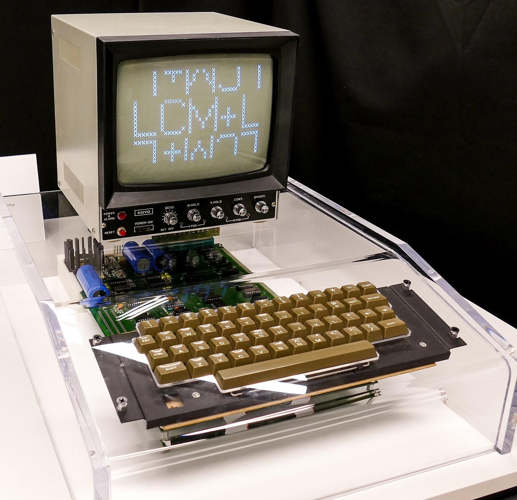
The Apple-1's display
The Apple-1 displayed 24 lines of forty characters on a television monitor. Like most computers at the time, the Apple-1 stored characters rather than pixels to reduce memory requirements. A character-generation ROM converted each character into a 5×7 matrix of pixels as it was displayed. To reduce memory even more, the display didn't store full bytes, but 6-bit characters, supporting upper-case letters, numbers, and some symbols.
The six-bit display characters were held in six 1024-bit shift registers. A seventh shift register tracked the cursor position.4 The diagram below shows the shift registers and the clock driver on the Apple-1 circuit board. These chips are in 8-pin packages, so two chips fit into the space of a regular TTL chip.5

The image below shows how the 2504 shift register chips are represented on the Apple-1 schematic. The chips use just 6 pins. Each chip has a single connection for bits coming in and a connection for the bits coming out. The remaining pins provide the two clock signals and the ±5 volt power supplies. Unlike RAM chips, these chips do not take an address.
PMOS integrated circuits
This shift register chip was created around 1970, an interesting time in the development of MOS integrated circuits. Early integrated circuits used a type of transistor known as bipolar. However, the metal-oxide-semiconductor (MOS) transistor had the potential to make cheaper, high-density integrated circuits. The first commercial MOS integrated circuit was a 20-bit shift register, created in 1964 by a company called General Microelectronics.
The diagram below shows the structure of a MOS transistor. At the bottom is the silicon, which is doped with impurities to form p-type silicon. The two conductive p-type regions are called the transistor's source and drain. The channel acts as a switch between the source and drain, turned on by voltage in the metal gate above. A thin insulating oxide layer separates the metal gate from the underlying silicon. These three layers—metal, oxide, semiconductor— give the MOS transistor its name. In the late 1960s, chips started to use gates made of polysilicon, a special type of silicon that produced better transistors than metal gates. This is the technology used by the 2504 shift register: the "P-MOS silicon gate process".
By the mid-1970s, however, integrated circuits changed in two more ways. First, P-MOS transistors were replaced by N-MOS transistors, which had better performance. Second, the introduction of ion implantation machines allowed transistor characteristics to be adjusted, with "depletion-mode" transistors8 leading to faster, lower-power circuitry. These changes ushered in the age of popular microprocessors such as the Zilog Z80, MOS Technology 6502, and Intel 8085. These had much better performance than earlier PMOS processors such as the Intel 8008.7 The 6502, of course, was the processor in the Apple-1 (and Apple II).
The shift register
Next, I'll look at the details of how the shift register was constructed. The idea of a shift register is that bits are passed from stage to stage, controlled by clock pulses. With 1024 stages, the shift register can hold 1024 bits. Each shift register stage uses two transistors and two inverters as shown below. During the first clock phase, the first transistor turns on, allowing the input bit to pass through it and the first inverter. During the second clock phase, the second transistor turns on, allowing the inverted value to pass through it and the second inverter, producing the output. Thus, a bit takes two clock phases to move through the shift register stage.
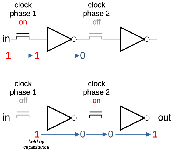
This circuit is a dynamic shift register, which works due to the circuit's capacitance. When the first transistor turns off, the value remains at the input to the first inverter, held by the capacitance of the circuit. (And likewise for the second transistor.) Because the gate of a MOSFET uses almost no current, the bit value will remain for a couple of milliseconds or so before it drains away. (This is the same principle used by DRAM, holding bits through capacitance.) As long as the clock keeps going, the bit gets refreshed by each stage.
Each inverter is implemented using two MOS transistors. The concept is shown on the left, below. A high input turns on the transistor, which pulls the output low. A low input turns off the transistor allowing the pull-up resistor to pull the output high. Thus, the circuit inverts its input.
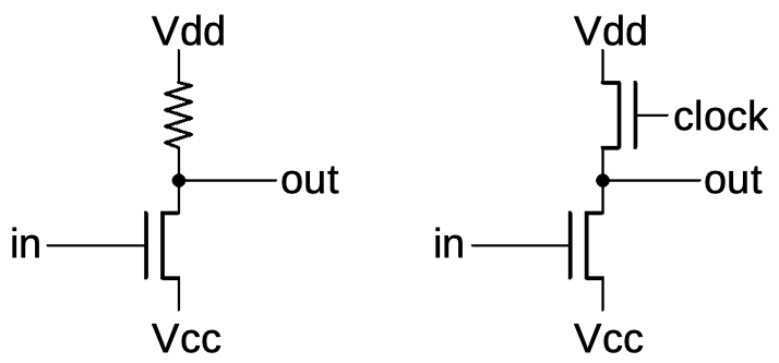
The circuit is actually implemented with a transistor in place of the resistor, as shown on the right, because transistors are more compact than resistors. A high input to the upper transistor turns it on, causing the pull-up current to flow. In a standard inverter, the transistor would be connected to be always on.9 However, the output of the inverter is only used during one clock phase. To reduce power consumption, the transistor is wired to the clock so it only acts as a pull-up when needed.
A shift-register stage on the die
The diagram below shows how shift-register stages are physically constructed on the die. The first part of the image shows how the circuitry appears under the microscope, a complicated jumble of silicon, polysilicon, and metal circuitry. In the middle, I've highlighted the doped silicon in green and the polysilicon in red. A transistor gate (yellow) is formed where polysilicon crosses silicon, with the source and drain on either side. (The horizontal metal wiring should be clear without highlighting.) Note the complex, optimized shapes of the polysilicon and the transistors. Finally, a black dot indicates a contact that connects two layers. In the bottom half of the image, bits are shifted to the right, while in the top half, bits are shifted to the left.
In the lower right, one stage of the shift register is represented by a schematic on top of the underlying circuitry. The stage is implemented with six transistors as described earlier. Note that the pull-up transistors to Vdd are long and skinny, reducing their current. The inverter transistors to Vcc, on the other hand, are wide, so they provide a lot of current. The circuitry in the top half of the image is the same, but rotated 180°. Note that the two rows of shift registers share the clock phase lines and Vdd, making the layout more efficient.6
Topology of the chip
You might expect the chip to consist of 1024 shift-register stages arranged into a chain. However, the chip had an unusual topology that allowed it to operate at double speed: one bit per clock phase instead of one bit per complete clock cycle. It accomplished this with a simple trick: it was really two 512-bit shift registers operating in parallel. The first operated on clock phase 1, phase 2, phase 1, ..., while the second was the opposite: phase 2, phase 1, phase 2, ... The result was that one half would produce bits in phase 1, while the other would produce bits in phase 2. The output circuit merged these together into a single output stream. From the outside, it looked like a 1024-bit shift register that operated twice as fast.
Another complication is that Signetics produced three 1024-bit shift register chips from the same silicon layout: the 2502 (organized as four 256-bit shift registers), the 2503 (512×2), and the Apple-1's 2504 (1024×1). The different chips were created by changing the metal wiring of the chip during manufacturing, which was much easier than building completely different chips. To support this, the shift register was broken into eight 128-bit segments, shown below. In the 1024×1 chip, two chains of four 128-bit segments ran in parallel (on opposite clock phases) to produce a 1024-bit shift register. The first chain used the light-colored segments A, B, C, D, while the second chain used the dark-colored segments. The segments are connected by the metal wiring along the side of the die. The chip's pads around the edges are labeled; the grayed-out ones are not used in this chip. The large block of circuitry above the output pin combines the two chains into one output.
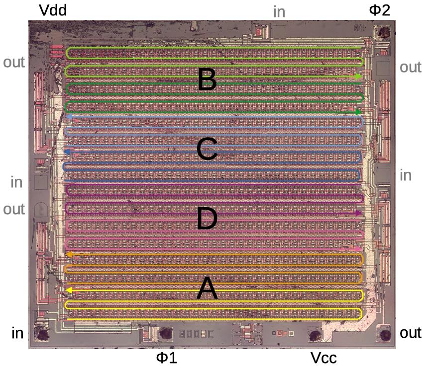
The other variants of the chip wire the shift-register segments differently and use additional input and output pins. The 512×2 2503 chip used four chains of 256 bits along with two input and output circuits. The 2502B chip used all eight 128-bit chains in parallel to form a 256×4 shift register, with four input and output circuits.10
The image below shows one of the unconnected outputs: the red polysilicon wire isn't connected at one end. With a small change to the metal layer, the metal wiring between two segments can be broken and the segment wired to this output instead. The other changes between chip versions are similar.
The clock driver
I'll wrap up with a brief mention of the clock driver chip that drives the shift registers. Shift-register memory chips required clock pulses with high current and unusual voltages due to the PMOS circuitry: from +5 volts to -11 volts. These pulses were provided by a special chip, the DS0025 Two-Phase MOS Clock Driver. The die photo below shows this chip. The die is dominated by four power transistors that produced 1.5 amp pulses. I wrote a blog post about the clock driver chip if you want more details.
Conclusion
The Apple-1 is now a collector's item, with boards selling for hundreds of thousands of dollars. However, when it was introduced in 1976, it wasn't a particularly important computer, with about 200 sold at the price of $666.66. The Apple II, which came out a year later in 1977, was a much more influential computer, selling millions to become one of the archetypical home computers of that era. The Apple II used RAM chips for all its storage, illustrating that shift-register memory had rapidly become obsolete.
The shift-register chip illustrates the amazing decline in memory prices, as reflected by Moore's Law. This 1-kilobit shift register cost about $60 (in current dollars), while a 16-gigabit DRAM chip now costs about $6. Thus, memory is about 160 million times cheaper now, an amazing drop.
I announce my latest blog posts on Twitter, so follow me @kenshirriff. I also have an RSS feed. Thanks to @TubeTimeUS for supplying the chip. I've written about the Intel 1405 shift register memory if you want to know more about this type of storage.
Notes and references
-
The first reference to the Signetics 2504 that I could find was in 1970, when each chip cost $11.05 in quantities of 100 (about $60 in current dollars). Looking in an old Byte magazine from 1976, a 1-kilobit shift register chip cost $9 ($34 in current dollars), while a 4-kilobit DRAM chip cost $20 ($75 in current dollars). Thus, it appears that even by the time the Apple-1 was released, DRAMs had become cheaper than shift registers.
The Apple-1 used 4-kilobit RAM for data and program storage. It's possible, though, to build a computer that uses shift-register storage for its main memory. The Datapoint 2200 is one example. If memory is accessed sequentially, shift-register storage is efficient since the bits are provided sequentially. However, if you access memory out of sequence, the processor has to wait while the memory cycles around, until the desired bits become available. In a way, shift-register memory is a throwback to very early computers such as EDSAC (1949), which used mercury delay lines for main storage. ↩
-
The behavior of shift-register memory was a good match for video circuitry, since characters are displayed on the screen in a fixed, repeating order (left to right and top to bottom). The IBM 2260 video display terminal (1965) used a technique similar to shift registers: it stored data in a sonic delay line, sending torsional pulses through a 50-foot nickel wire. But unlike the Apple-1, this delay line stored pixels, not characters. For more about this system, see my blog post. ↩
-
The die was encased in an epoxy package. To expose the die, Eric (@TubeTimeUS) tediously sanded through the plastic package until the die was visible. There are a few scratches on the die from this process, especially in the upper left. ↩
-
The display circuitry has some additional complexity. Characters can't be taken directly from the display shift register: since each character is made up of eight scan lines; a line of character must be processed eight times. To handle this, a second shift register (six 40-bit registers) buffers a line of characters and feeds each character into a display ROM. Another 1024-bit shift register keeps track of the cursor position. For more details, see stackexchange. ↩
-
The Apple-1 display has a lot of similarity with the popular TV Typewriter, a hobbyist video terminal kit from 1973. The TV Typewriter used shift-register memory for its 32×16 display, but had a complex 5-board design. Wozniak's design for the Apple-1 was much simpler. ↩
-
The schematic of the chip is shown below. Notice the upper and lower shift registers, which run on opposite clock phases. Apart from the 6-transistor shift-register stages, the only circuitry is the output stage that merges the two results and drives the output pin.
Schematic of the chip. Click for a larger image. From the 1972 databook. -
Another major improvement in integrated circuits was the introduction of CMOS, which used NMOS and PMOS transistors together, with much lower power consumption. By the 1980s, processors such as the Intel 80386 (1985) and Motorola 68030 (1987) used CMOS. CMOS is still used in modern integrated circuits. ↩
-
In the mid-1970s, ion implantation technology allowed the creation of depletion-mode transistors. These transistors could be used as pull-up elements, called depletion loads. Since depletion-load transistors could operate faster and with less current, they rapidly became a standard part of MOS integrated circuits, until replaced by CMOS in the 1980s. The Zilog Z80 and Intel 2102 SRAM were two early chips that used depletion loads. ↩
-
You might think that the inverter circuit will result in a short circuit between Vdd and Vcc when both the input and the clock are high. However, the pull-up transistor is designed to produce a weak current, so the other transistor can still pull the output low. This current results in relatively high power consumption for PMOS or NMOS circuitry, a problem that is fixed by CMOS. ↩
-
The 256×4 2502B chip required a 16-pin package, rather than the 8-pin package of other chips, due to the additional input and output pins. ↩
Recommend
About Joyk
Aggregate valuable and interesting links.
Joyk means Joy of geeK