

Reverse-engineering the LM185 voltage reference chip and its bandgap reference
source link: https://www.righto.com/2022/04/reverse-engineering-lm185-voltage.html
Go to the source link to view the article. You can view the picture content, updated content and better typesetting reading experience. If the link is broken, please click the button below to view the snapshot at that time.

Computer history, restoring vintage computers, IC reverse engineering, and whatever
Reverse-engineering the LM185 voltage reference chip and its bandgap reference
Many circuits, such as a computer power supply or a phone charger, require a stable voltage reference, but it's harder than you might expect to keep a voltage stable when the temperature changes. One integrated circuit that does this is the LM185.1 I looked at the die of this chip and found some interesting features. The same silicon die is used for three different integrated circuits, using tiny internal fuses to change its functionality. The chip uses a special circuit called the bandgap reference to keep the voltage stable even if the temperature changes. In this blog post, I'll discuss the circuitry of the LM185 and its implementation in silicon.
The photo above shows the LM185 die under the microscope, a tiny square of silicon. The underlying silicon is blue-gray, while the metal wiring on top is orangish. Regions of the silicon are doped with various impurities to form the transistors, resistors, and other devices on the chip. The variations in doping are visible as slight color changes in the silicon. At the top is the National Semiconductor logo.
The LM185 is available in three variants. The LM185-ADJ is the adjustable voltage reference. It has three pins: one is a feedback pin that controls the voltage. The LM185-1.2-N is a two-pin device, called a "micropower voltage reference diode". It is similar to a Zener diode providing 1.235V, but with better performance. (Lower power consumption, less noise, and better stability.) Finally, the LM185-2.5-N provides a 2.5V reference. The three variants are based on the same silicon die. The latter two have the feedback wired internally to provide a fixed voltage rather than an adjustable voltage.
The next sections describe how the various components of the chip are fabricated from silicon, and how they appear on the die.
NPN transistors
The photo below shows a closeup of one of the transistors in the LM185. The black lines and slightly different tints in the silicon indicate regions that have been doped to form N and P regions. The whitish areas are the metal layer of the chip on top of the silicon—these form the wires connected to the collector, emitter, and base.
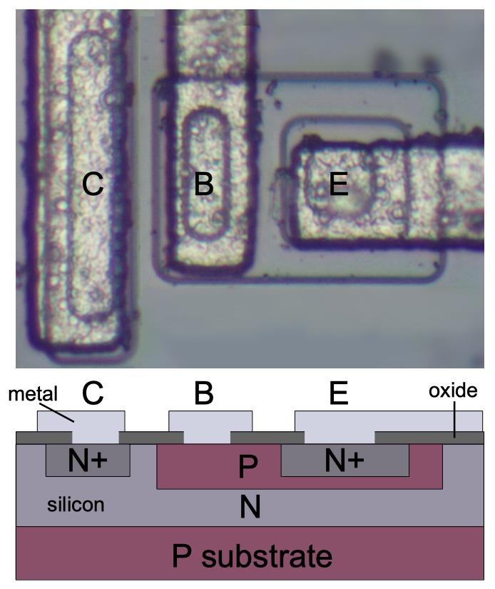
Underneath the photo is a cross-section drawing illustrating how the transistor is constructed. There's a lot more than just the N-P-N sandwich you see in books, but if you look carefully at the vertical cross-section below the 'E', you can find the N-P-N that forms the transistor. The emitter (E) wire is connected to N+ silicon. Below that is a P layer connected to the base contact (B). And below that is an N+ layer connected (indirectly) to the collector (C).
The output transistor (below) is much larger than the other transistors and has a different structure in order to support the chip's high-current output. It has multiple interlocking "fingers" for the emitter and base, surrounded by the large collector.
PNP transistors
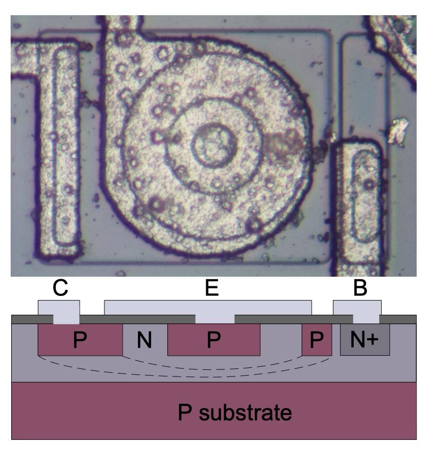
You might expect PNP transistors to be similar to NPN transistors, just swapping the roles of N and P silicon. But for a variety of reasons, PNP transistors have an entirely different construction. They consist of a small circular emitter (P), surrounded by a ring-shaped base (N), which is surrounded by the collector (P). This forms a P-N-P sandwich horizontally (laterally), unlike the vertical structure of the NPN transistors.
The diagram below shows one of the PNP transistors in the LM185, along with a cross-section showing the silicon structure. Note that although the metal contact for the base is on the edge of the transistor, it is electrically connected through the N and N+ regions to its active ring in between the collector and emitter.
Resistors
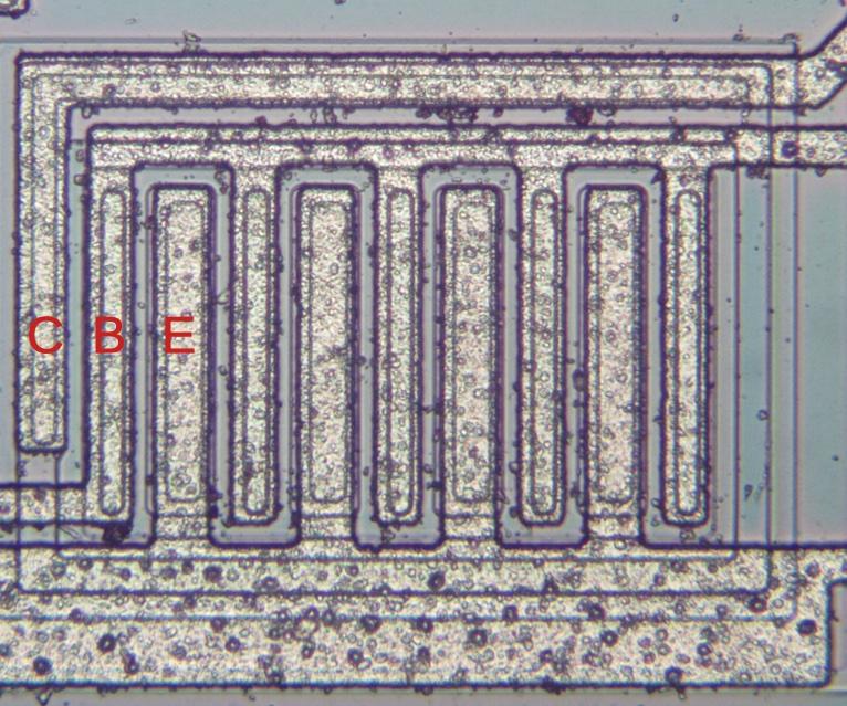
Resistors are a key component of analog chips. Unfortunately, resistors in ICs are large and inaccurate; the resistances can vary by 50% from chip to chip. Thus, analog ICs are designed so only the ratio of resistors matters, not the absolute values, since the ratios remain nearly constant. The photo below shows two paralleled resistors. Other resistors have a zig-zag shape to fit a longer resistor into the available space.
Capacitors
A capacitor consists of a metal plate on top of silicon, separated by a thin oxide layer that acts as a dielectric. Capacitors are fairly large on integrated circuits; they are the most visible components on this die. The capacitor below contains multiple circular patterns. These may be doped silicon regions, where the junction between two regions provides additional capacitance.
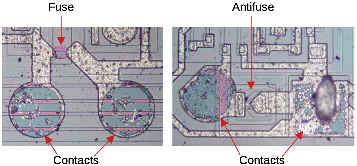
Fuses
Fuses allow the circuitry of the chip to be changed after manufacturing. The LM185 uses fuses for two reasons. First, fuses can add or remove resistance, allowing the circuit to be tuned for higher performance. Second, a fuse changes the feedback circuitry between the LM185-1.2-N and LM185-2.5-N variants. (The LM185-ADJ version requires more changes than are supported by fuses, so it needs some changes to the metal layer. For instance, it has three pads connected instead of two.)
A fuse has two metal pads attached. Before the chip is packaged, probes can contact the pads and apply a high current to blow the fuse. The first type of fuse is implemented with a tiny strip of metal that is vaporized to break the circuit, just like a large-scale fuse. The second type of fuse is an "antifuse", which has the opposite behavior: it does not conduct until a high current is applied, at which point it becomes conductive. The antifuse can be built from a Zener diode, and the process of shorting it out is called a "Zener zap". The high current forms metal spikes through the junction, causing it to permanently conduct. The diagram below shows a fuse and an antifuse as they appear on the die.
IC circuit: The current mirror
There are some subcircuits that are very common in analog ICs, but may seem mysterious at first. The current mirror is one of these. The idea is you start with one known current and then you can "clone" multiple copies of the current with a simple transistor circuit, the current mirror.
The following circuit shows how a current mirror is implemented with three identical transistors.2 A reference current passes through the transistor on the right. (In this case, the current is set by the resistor.) Since all the transistors have the same emitter voltage and base voltage, they source the same current, so the currents on the left match the reference current.
A common use of a current mirror is to replace resistors. As explained earlier, resistors inside ICs are both inconveniently large and inaccurate. It saves space to use a current mirror instead of multiple resistors whenever possible. Also, the currents produced by a current mirror are nearly identical, unlike the currents produced by two resistors.
Interactive chip explorer
To illustrate how the components form the chip, the die photo and schematic below are interactive. Click on a component in the die or schematic, and a brief explanation of the component will be displayed.
Because the three variants of the LM185 are slightly different, I had to combine three schematics to form the schematic above. Red components are only in the LM185-ADJ, green components are in the LM185-1.2-N, blue components are in the LM185-2.5-N, and cyan components are in the latter two chips. Note that the primary difference is the feedback circuit, but there are additional differences as well.
How a bandgap reference works
The main problem with producing a stable voltage from an IC is that the chip's parameters change as temperature changes. The bandgap voltage reference is commonly used to create a temperature-independent voltage reference.5 The trick is that it has one voltage that goes down with temperature and another than goes up with temperature. If you combine them correctly, you get a voltage that is stable with temperature.
To create a voltage that goes down with temperature, you can put a constant current through the transistor and look at the voltage between the base and emitter, called Vbe. The graph below shows how this voltage drops as the temperature increases. At the left, the line hits the bandgap voltage of silicon, about 1.2 volts; this will be important later.
If you set up a second transistor this way but with a lower current3, you get the same effect but the voltage Vbe curve drops faster. This may not seem helpful since we need a voltage that goes up with temperature. But here's the trick: if you subtract the two Vbe voltages, the difference increases as temperature increases, since the lines get farther apart. The difference is called ΔVbe. The graph below shows the Vbe curves for two different transistors, and you can see how the difference ΔVbe between the curves increases with temperature, even though both curves decrease with temperature.
The final step to a bandgap reference is to combine Vbe and ΔVbe in the right ratio so the result is constant with temperature. It turns out that if the values sum to the bandgap voltage of silicon (approximately 1.2 volts), the drop in Vbe and the increase in ΔVbe cancel out. In the graph below, adding 10 copies of ΔVbe is the right ratio; the exact ratio depends on the particular transistors. The important thing to notice in the graph below is that as the temperature changes, Vbe+nΔVbe remains constant - the top of the blue ΔVbe line remains at the bandgap voltage.
In the LM185, the key transistors are Q10 and Q11, where Q10 has 10 emitters in parallel, so each has 1/10 the current. Thus, if you feed the same current into both transistors, Q10 has a lower Vbe voltage than Q11 as described above. Note that Q10 is split in two: one half above Q11 and one half below Q11. This layout minimizes potential error due to a temperature gradient across the die. Half of Q10 will be hotter than Q11 and half will be cooler, so the difference will cancel out.
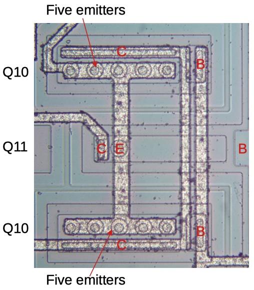
The diagram below shows how the bandgap reference is implemented in the LM185. Transistors Q10 and Q11 have different Vbe voltages due to their relative sizes. The difference in these voltages (ΔVbe) is developed across R7. Since the same current flows through R6, R7, and R8, the voltage across R6 will be 4ΔVbe and the voltage across R8 will be 6ΔVbe by Ohm's law. Thus, the combination of R6, R7, and R8 multiply ΔVbe by 11. Meanwhile, Q14 has its own Vbe.
Summing the voltages along the right gives Vbe + 11ΔVbe, which is designed to match the temperature-stabilized bandgap voltage of 1.2 volts. Thus, the circuit will be balanced4 if the voltage between the feedback input and V+ is 1.2 volts. If the voltage is not 1.2 volts, Q10 and Q11 will pass different amounts of current. Since the current mirror (Q12 and Q13) attempts to feed the same current into Q10 and Q11, any discrepancy will appear as current at the error output. This error current is amplified and controls the output transistor, adjusting the voltage until the feedback voltage is brought back into compliance. Thus, the circuit maintains the desired voltage, stabilized even if the temperature changes.
Conclusion
Well, that turned into a longer blog post than I was expecting. Although the LM185 doesn't contain many components by modern standards, it provides a stable, regulated voltage reference. It has some interesting features such as the use of fuses both to improve performance and to sell variant chips. It also illustrates the principle of the bandgap voltage regulator.
I announce my latest blog posts on Twitter, so follow me @kenshirriff. I also have an RSS feed. Thanks to Mitch Wright for supplying the chip.
Notes and references
-
The LM185, LM285, and LM385 are the same chip, but with different temperature ranges. The LM185 is rated for the military temperature range: -55°C to 125°C. The LM285 is rated for the automotive temperature range: -40°C to 85°C. The LM385 is rated for the standard temperature range: 0°C to 70°C. I believe the chips are identical except for testing. For the purposes of this post, you can treat the three chips as identical. ↩
-
For more information about current mirrors, check Wikipedia or chapter 3 of Designing Analog Chips. ↩
-
When building a bandgap reference, what really matters for Vbe is the current density through the transistors - the current divided by the area of the emitter. Decreasing the current through the transistor decreases the current density. The second way to decrease current density is to use a larger transistor with a larger emitter. Often five or ten identical transistors in parallel will be combined to form this large transistor to ensure the large transistor and the small transistor are exactly matched. ↩
-
One tricky thing about the bandgap circuit is that it is implemented "backward", taking the voltage as an input. The chip's block diagram6 shows that the reference generates 1.2 volts and this is compared to the input voltage. But in reality, the input voltage is fed into the bandgap circuit. If the input is 1.2 volts, the circuit is balanced. But if the input is too high or too low, the bandgap circuit will be unbalanced with more current through one transistor than the other. This "error" signal is amplified and used as feedback to adjust the input voltage until it matches 1.2 volts. In other words, there's no 1.2-volt reference inside the chip. Instead, the chip and its external input form a feedback loop that generates 1.2 volts. ↩
-
I've written before about bandgap references, specifically the 7805 voltage regulator and the TL431. ↩
-
The TL431 is a popular voltage reference, used in many power supplies. The main difference is that the LM185 regulates the voltage relative to the positive side, while the TL431 regulates the voltage relative to the negative side.
Comparison of the LM185 and TL431 block diagrams, from the datasheets.
Recommend
About Joyk
Aggregate valuable and interesting links.
Joyk means Joy of geeK