

Reverse-engineering the waveform generator in a 1969 breadboard
source link: https://www.righto.com/2022/03/reverse-engineering-waveform-generator.html
Go to the source link to view the article. You can view the picture content, updated content and better typesetting reading experience. If the link is broken, please click the button below to view the snapshot at that time.

Computer history, restoring vintage computers, IC reverse engineering, and whatever
Reverse-engineering the waveform generator in a 1969 breadboard
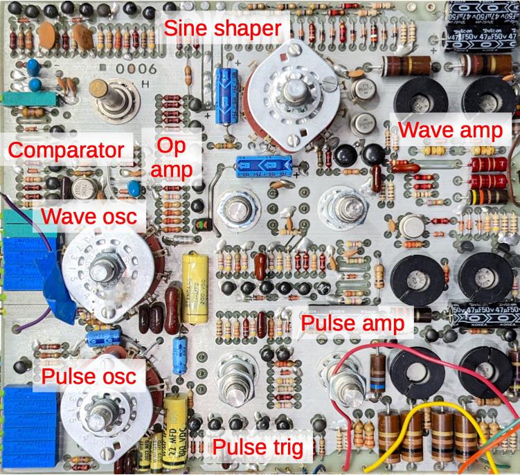
How hard could it be to fix a vintage solderless breadboard that doesn't quite work? The "elite 2 circuit design test system" below combined a solderless breadboard with some supporting circuitry: power supplies, a waveform generator, a pulse generator, switches, and lights. CuriousMarc found one of these breadboards on eBay, but the function generator didn't work, so we set out to repair it.
I figured that the waveform and pulse generators would be simple circuits, but they turn out to be implemented with a board crammed full of components, including over 40 transistors. I reverse-engineered the circuitry and found some interesting circuits inside, including op-amps implemented from discrete transistors. This complexity probably explains the shockingly high price of this breadboard: $1300 in 1969 (equivalent to $10,000 in current dollars).1
The waveform generator
The breadboard has a waveform generator that produces triangle, square, and sine waves over a wide frequency range, up to 1 megahertz. These waveforms are generated through a complex circuit that charges and discharges an integrator to produce the triangle wave. A comparator turns the triangle wave into a square wave. Finally, a sine-wave shaping network produces a sine wave from the triangle wave.
Triangle-wave generator
The oscillator's frequency is selected by resistors and capacitors. The faster the capacitor charges through the resistor, the higher the frequency. Thus, increasing the capacitance and resistance slows the oscillation. The frequency range knob turns a vintage wafer rotary switch to select one of seven different resistors and capacitors, allowing frequencies over a wide range from 1 Hertz to 1 megahertz. A potentiometer adjusts the frequency within the range to provide the exact desired frequency.
The triangle wave is generated from an op-amp integrator circuit, using the approach below. This circuit uses the capacitor to integrate the input voltage, producing the output voltage. The result is that the square wave input increases or decreases the output linearly, yielding a triangle wave. (The op-amp keeps that right side of R1 at ground, so the current that charges the capacitor is proportional to the input voltage. In contrast, in a simple R-C charging circuit, the capacitor charges exponentially; the charging current drops as the capacitor's voltage increases.)
To make an oscillator, the other piece is a comparator to provide the square wave input to the integrator. The comparator reverses direction at the top and bottom of the triangle wave, as shown below. When the input to the integrator is positive, the integrator output climbs linearly. This output is fed into the comparator, along with a limit level (red dots). When the output exceeds the upper limit at "A", the comparator output becomes negative. Since the comparator output is used as the integrator input, the integrator now discharges and the signal drops. When the signal drops below the limit at B, the comparator switches on and the process repeats. A hysteresis circuit changes the comparator level (dotted red line) at A and B, setting the upper and lower limits of the triangle wave.2
The comparator is a 710HC, a simple differential comparator integrated circuit introduced by Fairchild around 1965. This is one of just two integrated circuits on the board.3 The IC is packaged in an 8-pin circular metal can. This package was common at the time for analog integrated circuits, as the metal can provided shielding.
Op-amp
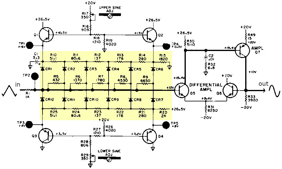
The op-amp is a key component of the integrator. Although integrated-circuit op-amps date back to 1963, this board builds op-amps out of discrete components. The integrator op-amp consists of seven transistors, along with a bunch of resistors and capacitors, as shown below. The heart of the op-amp is the differential pair (Q30 and Q32), a standard analog circuit. A fixed current is fed into the differential pair transistors. If one transistor has a slightly higher input than the other, that transistor turns on and most of the current will go through that transistor. Thus, the differential pair amplifies the difference between the inputs, the key function of an op-amp. Additional amplification is provided by Q33, while Q34 and Q35 buffer the dual outputs.
The output amplifier for the waveform circuit uses another discrete op-amp. This one has two stages of differential pairs for additional amplification, followed by power transistors to produce a high-current output. Another op-amp circuit is used in the sine-wave shaper, discussed below.
Sine-wave shaper
The board uses a surprising technique to generate sine waves: it synthesizes a sine wave from the triangle wave. Specifically, a resistor-diode network shapes the sine wave using piecewise-linear segments. The idea is to use diodes as switches that turn on as the signal level crosses various points. This adds resistance into the circuit, changing the slope. The result is a sine wave with less than 1% distortion.
The sine-wave shaper appears to be inspired by the similar circuit in the HP 3300A Function Generator, introduced in 1965. The schematic below shows the HP 3300A's sine-wave shaper; the breadboard's network is similar. The resistances are carefully chosen to achieve the sine wave. Similar resistor-diode networks were also used in analog computers to implement arbitrary functions, sometimes with user-adjustable resistances to change the function.
Pulse generator
The pulse generator produces pulses from 100 ns to 100 ms wide. These pulses can be triggered by the waveform generator, an external trigger input, or a "one-shot" pushbutton. The pulse width is controlled by a switch-selectable resistor-capacitor network.
The most unusual part of the pulse generator is how the output circuit adjusts the pulse amplitude. Instead of simply adjusting the amplification, the circuit changes the voltage that powers the output amplifier. This variable voltage is produced by an LM305 voltage regulator IC, adjusted by the amplitude knob on the breadboard. A four-transistor circuit produces the matching negative voltage.4 These voltages power a fairly complex output stage with two circuits. One circuit produces positive pulses, while the other produces negative pulses.
Conclusion
A prototyping breadboard may seem like a simple product, but everything becomes more complicated when built with 1969 technology. This breadboard includes a precision waveform generator and power supplies, designed for high accuracy, so it was almost like having test equipment included. But these features came at a steep price, equivalent to $10,000 today.
After I reverse-engineered the board,5 CuriousMarc used the schematic to fix the problems. The breadboard turned out to be in bad shape with a broken wire, a bunch of bad transistors, and a failed bridge rectifier in the power supply.6 It's unclear why the board had so many problems, more than you'd expect from age alone. Maybe the power supply over-voltaged the components at some point? My full schematic for the board is here.7
Follow me on Twitter @kenshirriff for more posts. I also have an RSS feed.
Notes and references
-
The hysteresis circuit is critical to the stability of the triangle wave. If the comparator input doesn't immediately switch to the lower level at "A", the comparator will switch again as soon as the integrator output drops slightly. Then the integrator will start rising, causing the comparator to switch again. The result is undesired high-speed oscillations (around a megahertz) with the triangle wave remaining stuck. This happened to us while attempting to repair the circuit when we replaced the hysteresis transistor with one that was a bit too slow. ↩
-
One unusual feature of the comparator chip is its asymmetrical power supplies. The positive supply (Vcc+) can go up to 14 volts, while the negative supply (Vcc-) is limited to -7 volts. This is inconvenient for the breadboard, which uses ±12 volt supplies internally. The solution is that the breadboard uses a 6.2-volt Zener diode to reduce the negative supply to the chip. R-C filters in the supply lines to the chip reduce noise. ↩
-
The negative-voltage circuit produces a negative voltage to match the user-selected positive voltage. In essence, it uses feedback from a resistor voltage divider between the positive and negative rails. When the two voltages are equal (and opposite), the voltage divider will yield 0 volts. If the voltages don't match, the signal from the voltage divider provides feedback to increase or decrease the negative rail as necessary. ↩
-
To reverse-engineer the board, I used a process that I've developed recently that works well. I took photos of both sides of the board and used the GIMP software to mirror one image and then align the images using the perspective tool. Next, I created a schematic in EAGLE, putting the symbols in their approximate locations. I wired up the schematic by drawing connections in EAGLE and marking the traces in GIMP as I handled them. The result of this was a "physical" schematic, approximately matching the board's layout.
The next step was to rearrange the components in EAGLE to create a more logical "functional" schematic. (I find that EAGLE works better than KiCad for this.) This schematic helped me understand how the circuitry was implemented, and we used it to trace through the circuitry and diagnose its problems. ↩
-
The breadboard has five different power supplies: three user-adjustable power supplies, and two supplies for internal use, providing unregulated ±32 volts and regulated ±12 volts. Modern systems typically use compact switching power supplies, but the breadboard uses two large and heavy power transformers. Five large power transistors provide regulation, along with massive capacitors. Overall, the power supply illustrates how much power supplies have improved since the 1960s. ↩
-
Disclaimer: the schematic isn't completely accurate. In particular, I didn't look up component numbers, so I'm kind of guessing on NPN vs PNP transistors and there are definitely errors. I also didn't record resistor and capacitor values. (The purpose of the schematic was to guide the repairs, not to completely document the device.) ↩
Recommend
About Joyk
Aggregate valuable and interesting links.
Joyk means Joy of geeK