

The magic of DC-DC voltage conversion
source link: https://lcamtuf.substack.com/p/the-magic-of-dc-dc-voltage-conversion
Go to the source link to view the article. You can view the picture content, updated content and better typesetting reading experience. If the link is broken, please click the button below to view the snapshot at that time.

The magic of DC-DC voltage conversion
Every other consumer electronic device on the market performs some form of DC voltage conversion. The reason is simple: the voltage you get out of a typical battery or a cheap wall wart is seldom right for every part of the circuit — from motors, to LCD backlights, to latest-generation digital chips.
Heck, your circuits might be doing voltage conversions without you knowing it. For example, a typical microcontroller will have a tiny internal charge pump to produce a higher voltage for EEPROM and flash memory. It might also have another regulator to produce a lower voltage for the CPU core.
Despite this, voltage conversions remain black magic to most enthusiasts. Antiquated linear ICs, such as LM7805 or LM317, crop up next to ultra-modern 32-bit MCUs. And if a switching regulator makes an appearance in a hobby project, the design is usually copied from elsewhere, with no regard to its suitability for the task at hand.
Today, let’s have a closer look at the task of converting DC voltages. These circuits are usually explained using complex terminology and dizzying math, but their operation is not hard to grasp.
Resistor-based voltage dividers
Let’s start from the beginning. The simplest way of deriving an intermediate voltage from a known, stable supply is to use a resistor-based voltage divider. The fundamental circuit, which should be familiar to most hobbyists, is shown below:
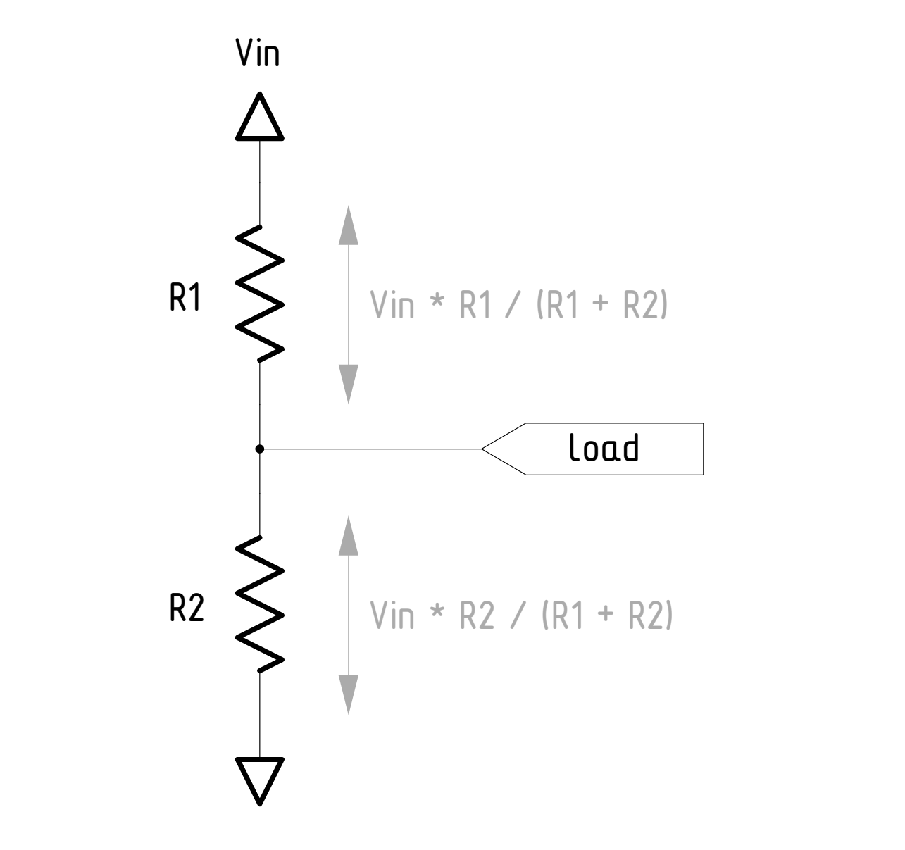
With no substantial load connected in the middle, the currents through R1 and R2 are equal, and each resistor develops a voltage drop proportional to the ratio of their resistances. In particular, if R1 = R2, the voltage at midpoint will be Vin/2. Easy enough.
The most severe limitation of this circuit is that it works correctly only if the current sourced through the “load” leg is negligible in proportion to the current flowing via R1 and R2; as soon as this condition is violated, the voltage in the middle begins to depend on what the load is doing too. It follows that impractically low resistances would be needed to supply stable voltages to power-hungry loads, resulting in high waste currents through the R1-R2 path.
In practice, it’s most common to encounter resistor-based dividers as bias networks for biasing op-amp inputs or FET gates. In such applications, the loading is practically nil, and the resistances can hover around 10 kΩ to 100 kΩ, resulting in microamp-range waste.
A somewhat more efficient variation of the traditional voltage divider can be constructed if the load heaves more or less like a constant resistance under the conditions encountered in the circuit. In such a case, the load itself can be made into a part of the divider in place of R2:

The first issue with this design is that it still wastes energy, just not as much as before. The reduction in voltage across the load is achieved by having R1 impede the flow of electrons, converting portion of the supplied energy into heat. The amount of waste heat is given by Joule’s law: P = IV. The losses become severe if the current is substantial and the required voltage reduction is more than a fraction of a volt.
The other gotcha of this topology is that relatively few loads behave like constant resistances while still doing something useful. In particular, neither an integrated circuit executing a program nor a motor under load would fit that bill. The current they require — and hence, their apparent conductivity / resistivity — changes over time. Because the operation of the divider depends on the ratio of resistances, the resulting voltage is bound to be thrown out of whack.
Basic linear regulators
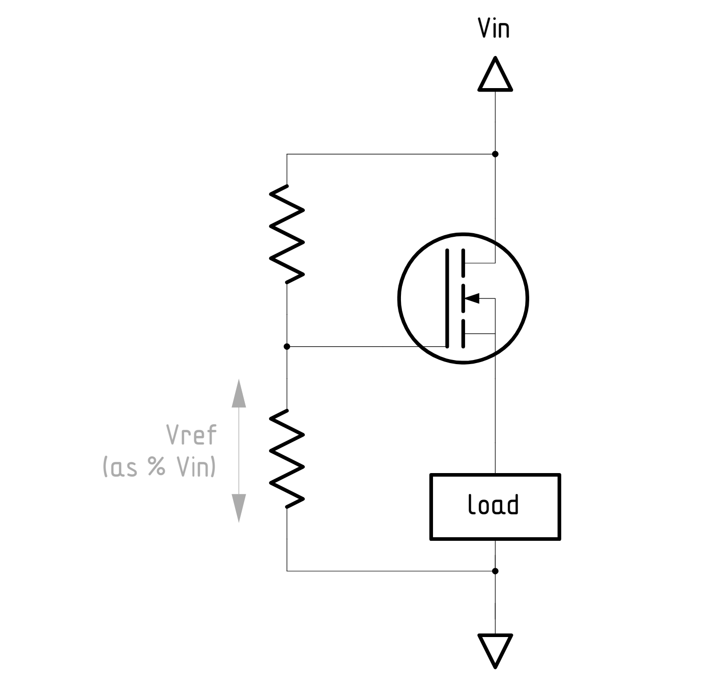
One solution to the challenge posed by variable-resistance loads is to make R1 variable too. One could imagine some sort of a feedback-based resistive circuit that conducts as much as little as needed to maintain a fixed ratio of resistances, and thus a consistent voltage across the connected load.
Well, those who remember an earlier article on signal amplification might recall that this description matches the behavior of a transistor-based voltage follower. In essence, an n-channel MOSFET conducts only if there is a sufficiently positive voltage between its source and gate terminals (Vgs > Vth). If we use a resistor-based voltage divider to supply the desired voltage to the gate terminal of such a transistor, and then place the load on the source side, we might get our wish:
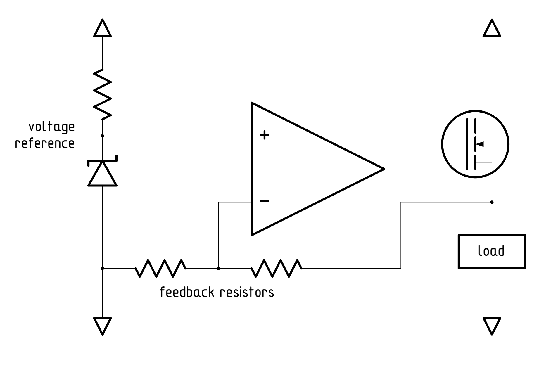
This circuit, which can be implemented with a general-purpose MOSFET such as 2N700, is not going to perform particularly well in practice — but within some bounds, it illustrates the basic operating principle of linear regulators. One of the first improvements we could attempt is to ditch resistors in favor of an internal Zener diode to provide an absolute voltage reference. A simplified example is:

The idea here is that a diode, if subjected to a controlled current flowing through it, develops a more or less constant voltage drop across its terminals as a consequence of the effort needed for electrons to power through the p-n junction depletion zone. In other words, within some sensible limits, the derived Vref is stable even if the supply voltage fluctuates over time.
To make this design behave better, we would also insert an operational amplifier that actively compares the output voltage to the reference, amplifies the difference by some reasonable amount (perhaps 10x), and then shifts the voltage at the gate of the transistor in the right direction until the error goes away. This approach helps alleviate some of the less-than-ideal I-V characteristics of the single-transistor design:
Either way, the deal with linear regulators is that despite what some internet sources might say, you probably shouldn’t be using them in your designs — not unless some exceptional circumstances apply. A fancy variable resistor is still a resistor: the energy is still being wasted in proportion to I and V. Between the resulting thermal management issues and reduced battery life, linear regulation is seldom worth the pain.
Switched capacitor converter (charge pump)
Switched-mode regulators are often thought as complex, but their operating principle is easy to explain. Let’s start with the following schematic, consisting of a freely-moving “flying” capacitor (Cf) and an output cap (Co):

If we connect Cf to the supply rails, as shown above, the capacitor will be charged and will develop a voltage equal to Vin across its terminals. This voltage is a consequence of a charge stored in the capacitor’s internal electrostatic field, and will persist if we disconnect it from the supply. You can take that capacitor and power some completely unrelated circuit at the same voltage for a brief while.
So, let’s take our charged Cf and connect it across the output cap:
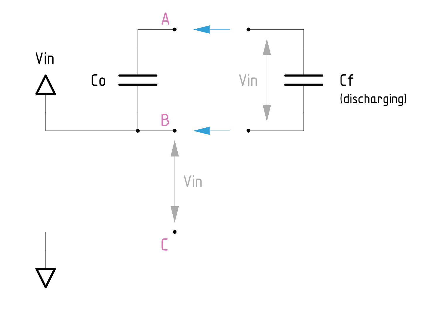
At that point, assuming that Co was initially discharged, Cf will transfer some of its charge to Co, producing a positive voltage across the terminals of the output cap. If this process is repeated a number of times, Co will become nearly fully charged, and a voltmeter will read something close to Vin between points A and B.
Note, however, that the output capacitor has its more negative terminal (B) tied to the positive supply rail. In an open circuit, this doesn’t permit any current to flow, but it means that if we connect a voltmeter across A and C, we will actually measure 2 × Vin. Huh — we have a voltage multiplier!
Of course, in a real charge pump, the flying capacitor is not physically moved; instead, it is electrically switched between these points using four field effect transistors toggled in a carefully choreographed sequence. The switching usually happens at a frequency between 100 kHz and 2 MHz, mediated by a supervisory circuit and facilitating near-seamless energy transfer to connected loads. Although these supervisory functions can be achieved in a number of ways, an increasingly common architecture is a simple microcontroller running a tiny bit of code.
Different arrangements of output capacitors can be used to achieve different multiplication ratios or to create negative voltages (that last part is done by dangling Co from the ground rail and flipping Cf back and forth). Heck, because the charge transfer process is symmetrical, it’s also possible to divide voltages using the same approach.
Because capacitors are very good at containing their internal fields and because modern multilayer ceramics (MLCCs) exhibit low impedances at standard charge pump operating frequencies, converter ICs such as LM2776 deliver excellent efficiency — often above 85% across a wide range of loads — without a whole lot of radio frequency interference.
On the flip side, a major limitation of simple charge pumps is that they lack voltage regulation: the device can produce arbitrary multiples of Vin, but if the supply fluctuates, so does the output of the converter. That said, because the flying capacitance is usually chosen to be smaller than the output capacitor, the charging of Co is stepwise, and some crude regulation can be achieved by monitoring the output voltage and varying the timing of the process. Alternatively, better but less efficient regulation might involve resistively limiting the current supplied to Cf to gain finer-grained control over its charge state. An example of a step-up charge pump regulated to about +/- 5% is LTC3240 — and as can be seen in the datasheet, overall efficiency takes a hit.
Other than a limited degree of voltage regulation, the main downside of charge pumps is their inherently discontinuous operation: there is never a direct flow of current from the supply to the load. This, coupled with the relatively high number of transistors in the charge transfer path, means that it’s unusual to see charge pumps designed for currents above 300 mA. Past that point, inductor-based designs take lead.
Buck converter
The simplest inductor-based voltage regulator is the buck converter. It is used to produce a tightly-controlled output voltage lower than the supply. The first part of the circuit is the following arrangement:
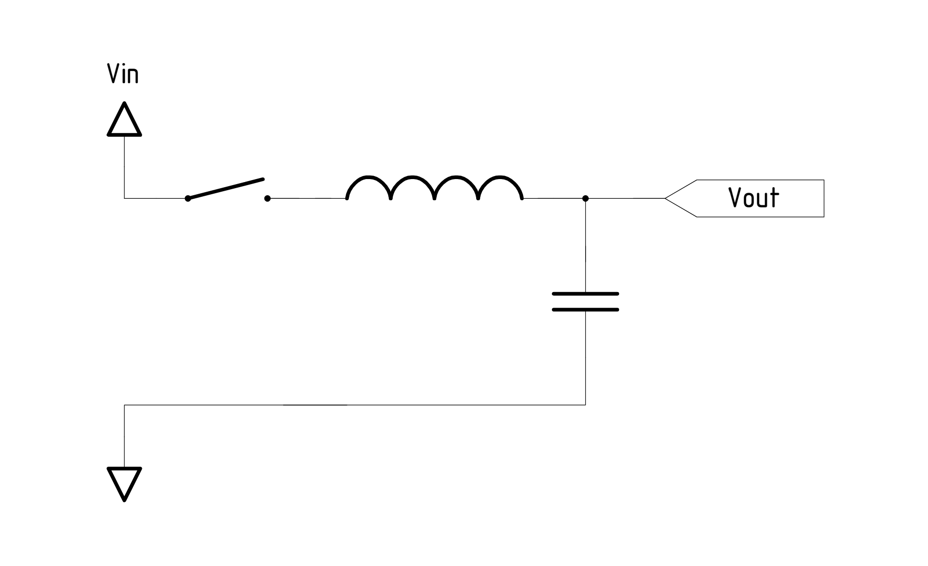
In essence, the controller of a buck converter monitors the output voltage and turns on the switch to recharge the output capacitor from the supply rail whenever the output voltage drops below the preset level.
Without some way to limit the inrush current, this circuit could behave erratically: the capacitor could charge too quickly, causing Vout to instantly overshoot all the way to Vin. A small resistor in the path of the charging current could be a solution, but it’s a somewhat wasteful affair. An inductor, which resists the change in current by reversibly diverting some of the energy into an internal magnetic field, seems like a better choice.
When the switch is first closed by the supervisory circuit, the current through the inductor ramps up gracefully, giving us good control over the charge level of the capacitor. But when the switch is opened down the line, a new problem arises: the collapsing magnetic field of the inductor releases the stored energy by continuing to push electrons down the path they were traveling before. In the absence of some new route for them to follow, this phenomenon creates a dangerous spike in voltage across the terminals of the inductor: negative on the switch side and positive on the capacitor side. Even worse, it causes the energy stored in the field to be unproductively dissipated, making the inductor no better than a resistor after all.
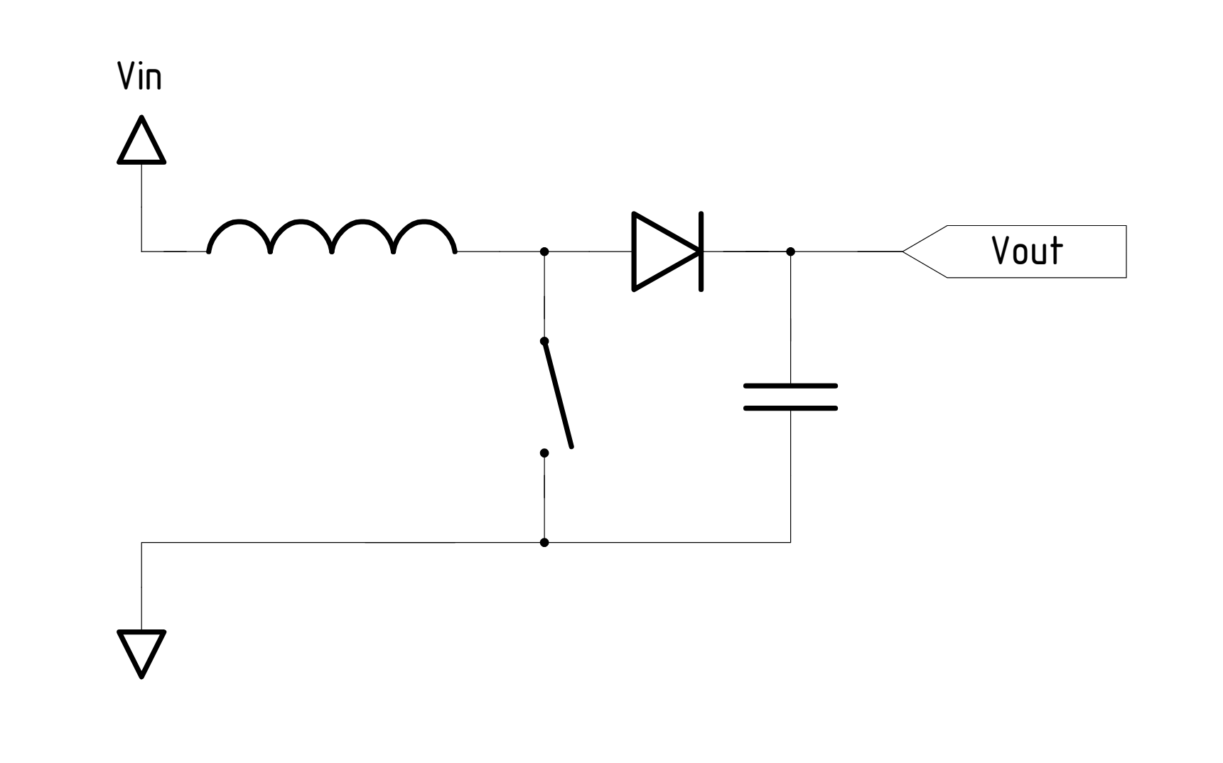
To address this problem, our simple buck converter must also incorporate a cleverly placed reverse-biased diode. The diode begins conducting once the left side of the inductor becomes more negative than the 0 V rail, which can only happen when the switch is open. With the diode conducting, electrons can be pulled by the collapsing magnetic field from the 0 V rail and pushed toward the capacitor and the load, where they will eventually find a productive return path:

Of course, this extra “switch break” current must be accounted for by the designers of the regulator to prevent overcharging the capacitor. That said, because the energy stored in the field is more or less proportional to the “on” time of the inductor, the magnitude of the phenomenon is easy to forecast and control.
Buck converters advertise high switching efficiencies, but they usually reach optimal performance only across a narrow range of loads. One major source of losses is the resistance of the inductor coil; this can be high especially if the element is chosen for low cost and the smallest possible footprint on the PCB. Another source of losses is the leakage of electromagnetic fields from the inductor, also causing MF and HF band radio interference — and making switched supplies mildly problematic in certain applications, such as radio receivers or precision amplifiers.
On the flip side, buck converters operate semi-continuously, with a direct path of current from the supply to the load; this means that they can effortlessly deliver high currents, and even tiny devices such as AP63203 can tackle several amps. The gradual ramp-up of current through the inductor also means excellent voltage regulation can be achieved without breaking a sweat.
It is perhaps worth noting that in addition to ICs that require external inductors, it’s also possible to buy inexpensive one-piece modules that require less tinkering and simplify circuit design. Two good examples are CUI VXO7803-500 and Murata mEZD71202A-F.
Boost converter
As discussed in the previous section, a limitation of the buck regulator is that the device can only output voltages lower than the supply rail. To produce higher voltages, it is necessary to take a different approach — and the most common route is the so-called boost topology:
Let’s consider what happens when the switch is closed. In principle, this creates a short-circuit between the supply rails — but for a brief while, the inductor resists the flow of current while diverting the energy of the supply into an internal magnetic field. Of course, this effect tapers off quickly, so to avoid a real short-circuit, the switch needs to be opened before long.
Once that circuit is broken, the collapsing magnetic field of the inductor tries to sustain the flow of charges in the direction they were flowing before. As in the case of a buck converter, this pushes the left terminal of the coil more negative, and makes the right terminal more positive.
Of course, the more negative side is still connected to the positive supply rail, so its potential remains constant in relation to the supply; meanwhile, a voltmeter connected to the other terminal would show a voltage higher than Vin. This voltage spike causes the diode to start conducting, permitting energy transfer to the capacitor.
Critically, because the peak electromotive force that can be generated by the coil far exceeds Vin, the capacitor can be charged to a higher voltage too. In fact, if the process is allowed to continue indefinitely, the capacitor could reach hundreds of volts. It follows that output regulation is critical. It can be achieved by varying the “on” time of the inductor, and thus the amount of energy transferred in each step.
Boost converters, such as MCP1642B/D, are commonly used to power higher-voltage devices from single alkaline cells, or to generate 10V+ for devices such as LCD backlights. The devices share most of the advantages and disadvantages with the buck topology: they require inductors and have a large RFI footprint, but can deliver fairly substantial currents with ease.
For earlier articles on electronics, click here.
Recommend
About Joyk
Aggregate valuable and interesting links.
Joyk means Joy of geeK