
7

红外摄影师分享英特尔酷睿i9-13900K透视图:展示Raptor Lake-S芯片结构
source link: https://www.expreview.com/85301.html
Go to the source link to view the article. You can view the picture content, updated content and better typesetting reading experience. If the link is broken, please click the button below to view the snapshot at that time.

红外摄影师分享英特尔酷睿i9-13900K透视图:展示Raptor Lake-S芯片结构
吕嘉俭发布于 2022-10-26 11:28
本文约 460 字、4 张图表,需 1 分钟阅读
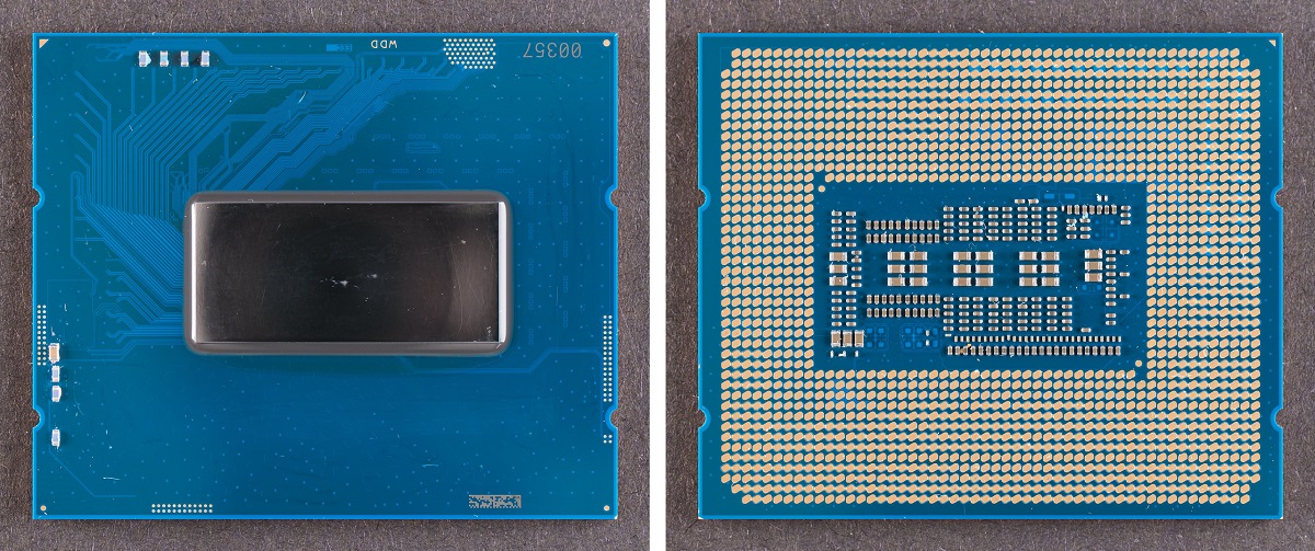
英特尔酷睿i9-13900K是新一代酷睿里的旗舰型号,拥有24核心及32线程,8个P-Core加上16个E-Core,L3缓存为36MB,P-Core最高睿频为5.8GHz,E-Core最高睿频为4.3GHz,PL1和PL2分别为125W和253W,采用Intel 7工艺制造。
近日,著名红外摄影师Fritzchens Fritz通过红外显微镜,展示了酷睿i9-13900K处理器内部的构造。
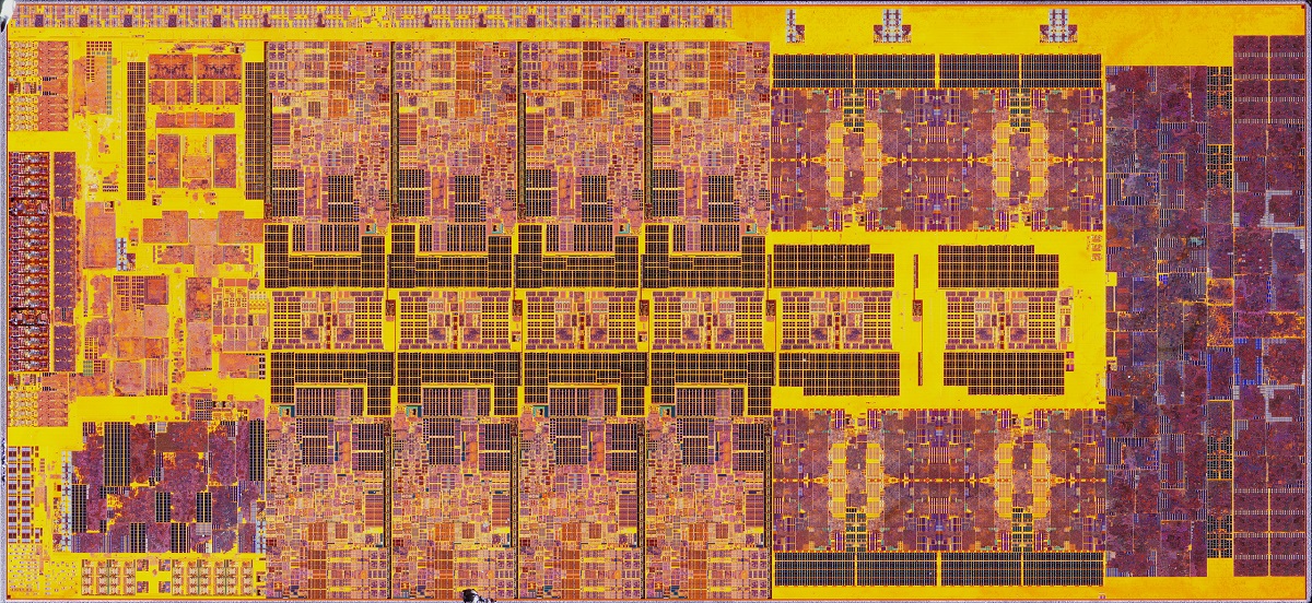
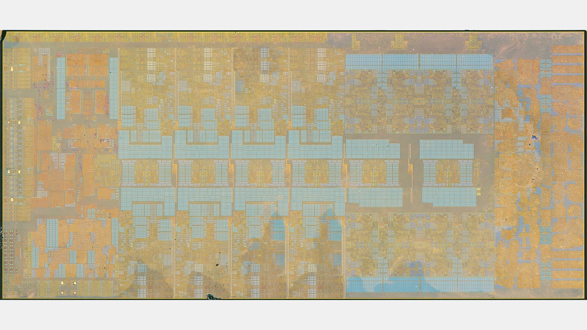
Raptor Lake-S的核心面积为252.65mm2,而上一代Alder Lake-S的面积为215.25mm2,更多的E-Core和增大的L2/L3缓存,使得相同工艺下的芯片面积增加,成本也会更高。在不计算L2/L3缓存的情况下,P-Core的面积为7.429mm2,E-Core的面积为1.58mm2。
Raptor Lake-S和Alder Lake-S两者有许多的共同点,比如使用环形总线让内核与图形引擎、I/O接口和内存控制器互联。P-Core分成两列排列,E-Core则被分成四组,每组为4个内核。
英特尔酷睿桌面处理器参数表
| 规格 | Coffee Lake-S | Comet Lake-S | Rocket Lake-S | Alder Lake-S | Raptor Lake-S | Meteor Lake-S | Arrow Lake-S | Lunar Lake-S | Nova Lake-S |
|---|---|---|---|---|---|---|---|---|---|
| 发布年份 | 2018 | 2020 | 2021Q1 | 2021Q4 | 2022 | 2023? | 2024? | 2024+? | 2026? |
| 工艺节点 | 14nm | 14nm | 14nm | Intel 7 | Intel 7 | Intel 4 TSMC N5? | Intel 4 & 20A TSMC N3? | Intel 18A TSMC N2? | TBC |
| 核心架构 | SkyLake | SkyLake | Cypress Cove | Golden Cove Gracemont | Raptor Cove Gracemont | Redwood Cove Crestmont | TBC | Lion Cove Skymont | Panther Cove Darkmont |
| 核显 | Gen9.5 | Gen9.5 | Gen12 | Gen12 | Gen12 | Gen 13? | TBC | TBC | TBC |
| 最大核心数 | 8 | 10 | 8 | 16 (8+8) | 24 (8+16) | TBC | 40 (8+32) | TBC | TBC |
| 插座 | LGA1151 | LGA1200 | LGA1200 | LGA1700 | LGA1700 | LGA1851 | TBC | TBC | TBC |
| 内存支持 | DDR4 | DDR4 | DDR4 | DDR4/5 | DDR4/DDR5 | DDR5 | TBC | TBC | TBC |
| PCIe版本 | PCIe 3.0 | PCIe 3.0 | PCIe 4.0 | PCIe 5.0 | PCIe 5.0 | PCIe 5.0? | PCIe 5.0? | PCIe 5.0? | PCIe 6.0? |
| 主板芯片组 | Intel 300系列 | Intel 400系列 | Intel 500系列 | Intel 600系列 | Intel 700系列 | TBC | TBC | TBC | TBC |
| 超 能 网 制 作 (展开) |
Recommend
About Joyk
Aggregate valuable and interesting links.
Joyk means Joy of geeK