

GaAs Thin Wafer的强度提升探究
source link: https://www.eefocus.com/component/520814
Go to the source link to view the article. You can view the picture content, updated content and better typesetting reading experience. If the link is broken, please click the button below to view the snapshot at that time.

上几天研究了一下GaAs的抛光,其实化合物半导体的抛光都会面临薄晶圆强度小,晶圆有着天然的解离镜像,容易裂片的问题。
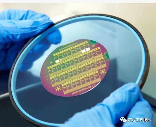
图片来源于网络
如上图,如果发生晶圆裂片,经常四分五裂,就这能做报废处理。
如何提高晶圆的强度,如上文提到的降低晶圆表面粗糙度可以提高。
如何实现呢?
早起大家研究的有两种方法,第一个是通过减薄之后的抛光,把磨砂面变成镜面,其实就是降低表面粗糙度,另外一个是腐蚀。今天找到一篇做的对比得论文,我们探究一下。
The study was done on the four-inch<100>GaAs wafers. The wafers were measured so that the total thickness variations (TTV) before and after grinding were less than 5 microns. All wafers were wax-mounted on the sapphire disk by the Logitech bonding machine.
TTV小于5um。
采用GN研磨设备。
The wet etch recipe used for this test was: 1(36.5% HCl): 4 (30% H2O2): 40 (DI), with an etch rate of about 0.3 microns per minute at room temperature.
the test wafers were loaded on the 12” Lap Master polishing machine. The wafer was rotated on the polishing pad. Polishing slurry was supplied to the pad and the removal rate was 1.2 microns per minute.
腐蚀和抛光工艺采用以上参数。
制备五个样品
1)减到100um的毛坯wafer
2)减到105um的然后腐蚀5um,
3)减到110um,然后腐蚀10um。
4)减到115um,然后腐蚀15um。
5)减到110um,然后抛光10um。
The Wafer Strength Measurements were taken by using an AIKO material strength tester manufactured by AIKO Engineering Inc. in Japan.The accuracy of the wafer strength measurement is+/- 0.01 lbs. 应力测试设备和精度要求。
urface roughness (Ra) [*]measurements by Chapman machine (model MP2100 non-contact measurement system)
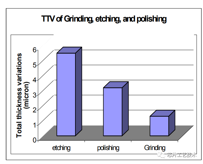
1、3、5三个waferTTV对比,Etching的最差
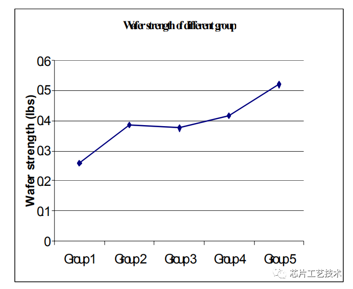
抛光的5号样品强度大


The lowering of surface roughness is a major factor for wafer strength improvement, the smoother is the surface, the stronger is the wafer. The smooth surface will help preventing breakage during the wafer demounting and solvent cleaning. It is very important to do polishing instead of wet etching process in the wafer thinning operation to minimize the thickness variation, and reduce the surface roughness to improve the wafer strength. By implementing the polishing process in our high volume production line the wafer breakage rate was reduced from 9.13% to 0.59%.
总的来说,多抛光,或者在抛光过程中,加入化学腐蚀的作用,比如加双氧水等。
版权声明:与非网经原作者授权转载,版权属于原作者。文章观点仅代表作者本人,不代表与非网立场。文章及其配图仅供工程师学习之用,如有侵权或者其他问题,请联系本站作侵删。 侵权投诉
Recommend
About Joyk
Aggregate valuable and interesting links.
Joyk means Joy of geeK