

Look inside the Raspberry Pi Zero 2 W and the RP3A0-AU
source link: https://www.jeffgeerling.com/blog/2021/look-inside-raspberry-pi-zero-2-w-and-rp3a0-au
Go to the source link to view the article. You can view the picture content, updated content and better typesetting reading experience. If the link is broken, please click the button below to view the snapshot at that time.

Look inside the Raspberry Pi Zero 2 W and the RP3A0-AU
October 28, 2021
Today, Raspberry Pi released their new Zero 2 W, and it includes a new Raspberry Pi-branded chip, labeled RP3A0-AU.
I was able to get early access to the Zero 2, and I have a full review of the device on my YouTube channel, but I wanted to share more of the X-ray images I took of the device to reveal its inner workings, and because I just think they look cool. Also, I paid a bit of money to get these pictures, so might as well share!
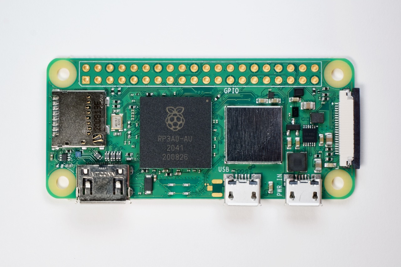
First, here's what the Zero 2 W looks like in person:
And here's what it looks like via X-ray:
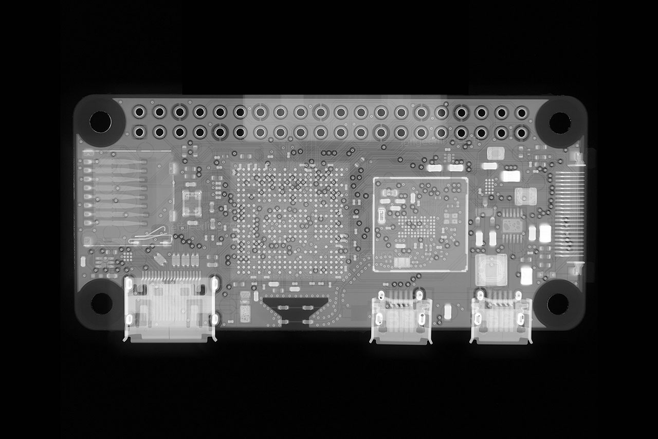
You might already see a few of the easter eggs hidden inside, but let's first get the basics out of the way. This board has the exact same physical layout as the earlier Pi Zero W, with the same I/O, meaning it will fit in almost every accessory and project designed for earlier Pi Zero models.
For I/O, it features:
- 1x mini CSI connector on edge for Pi Camera modules
- 1x microSD card reader for boot volumes
- 1x micro USB power input
- 1x micro USB data port
- 1x mini HDMI display port
- 40-pin GPIO (following standard Pi layout)
But looking more closely at the X-ray image reveals what's inside the new Pi chip:
You can distinctly see two sets of bond wires—in this case, gold bond wires, as indicated by the -AU chip suffix—with one leading to the 512MB LPDDR2 RAM on top, and the other leading to the BCM2710A1 clocked at 1 GHz on the bottom.
So this is not custom silicon, but it is a custom 'package'. Older Pi Zero models (and some of the older Pi A/B models) used a package-on-package layout, but the BCM2710 used here didn't come in a variety that was stackable. So Raspberry Pi decided to make their own, and put it all inside one easier-to-mass-produce chip.
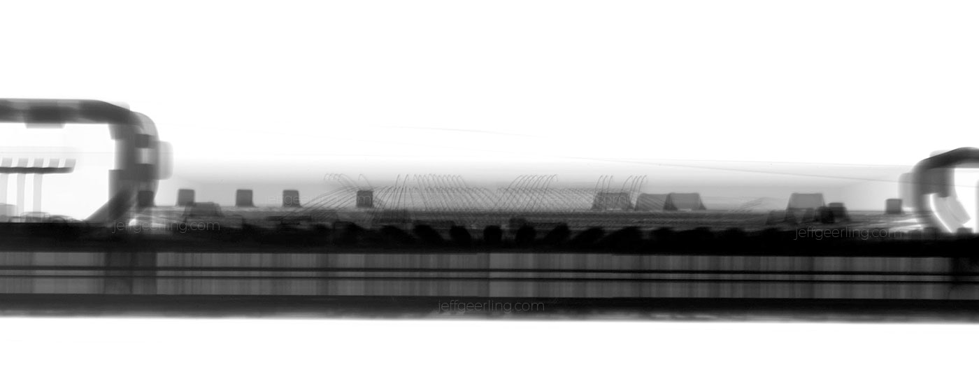
But I was looking through more angles via digital X-ray when something else caught my eye:
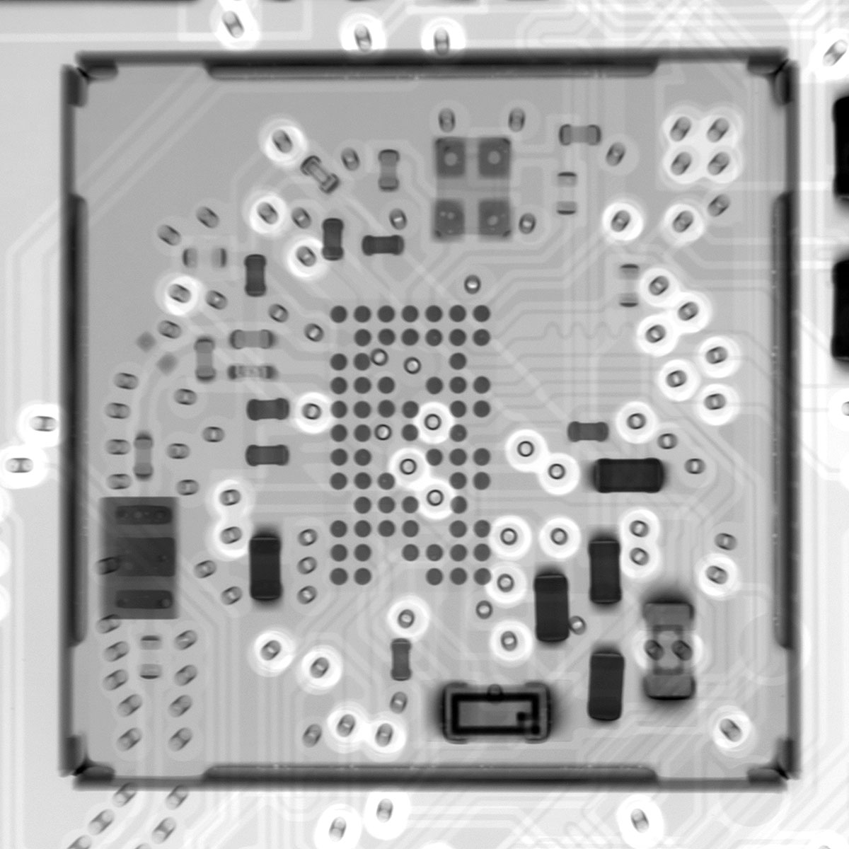
Do you see that little pattern in the middle of the BGA ('Ball Grid Array') on the main chip? Does it remind you of anything? How about we zoom and enhance:
And there it is! I stuck a transparent Pi logo on there in case it's still hard to see. I love seeing little design details like this, since it reminds me of the signatures inside the Macintosh case—a little mark of pride from the hardware designer that also shows a spirit of playfulness... and in a place where vanishingly few people will ever notice!
I had to know more, so I asked Gordon Hollingworth about the design, and he referred me to Simon Martin, who was principle designer of this chip. He was happy to see someone noticed, and had a bit to say:
The BGA ballout is just a bit of fun. The balls on the outside of the package contain the I/O signals and have to be carefully placed. The balls in the middle are just power and ground (and help with cooling) so can be placed in any arrangement.
I also asked a bit more about the chip design since, well, he designed it! And he mentioned that the SoC and DRAM have a silicon spacer to make sure the bond wires aren't crushed during manufacturing. And he also mentioned why they chose gold bond wires:
It's a busy looking thing if viewed under X-Ray. Over 800 gold bond wires [...] We got a bit scared of using cheaper copper wires in the package and decided on the gold version to ensure a long life.
So there you have it! I also wanted to take a peek under the WiFi/Bluetooth module cover, to see what's inside, and it's very similar to the older board, just encased inside a metal shield:
I'll get more into this next week, but the actual chip used here is the SYN43436, made by Synaptics. It's very close to the BCM43438 used in the 3 model B and Zero W, but it does require dedicated firmware, and that threw me for a loop while working on a RetroPie build for the Zero 2 W!
Anyways, that about sums up the 'inside look' at the Zero 2 W—please check out my YouTube review of the Raspberry Pi Zero 2 W for more juicy design details.
Performance
To help those who don't enjoy sitting through videos, I'm also posting the performance benchmarks here:
I ran all these benchmarks using my pi-general-benchmark script, and this first one was interesting—due to the fact the Pi Zero W and Zero 2 W have 512 MB of RAM, it was hard to even get the benchmark to complete. The OOM (Out Of Memory) Killer was ruthless in killing the runs until I gave the Pi at least 512 MB of swap space on the slow microSD storage.
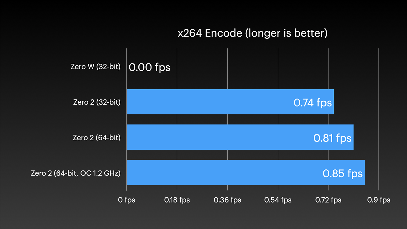
It's not showing a ton of speed, but another thing to note is the Pi Zero 2 can take an overclock of 1.2 or even 1.4 GHz with adequate cooling. I get more into thermals and efficiency in my video, but moving on to the next benchmark, the following become apparent:
- The Pi Zero 2 W is 2x faster at base clock on 32-bit Pi OS.
- The Pi Zero 2 W can finally run 64-bit Pi OS.
- The Pi Zero 2 W can be 3-4x faster (or more!) running 64-bit Pi OS with a slight overclock.
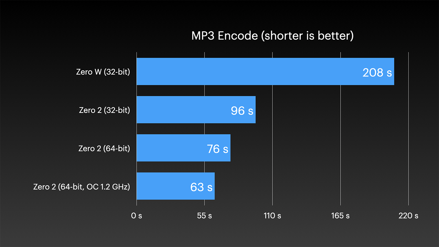
Here's the result of an MP3 encode test:
And finally, phpbench:
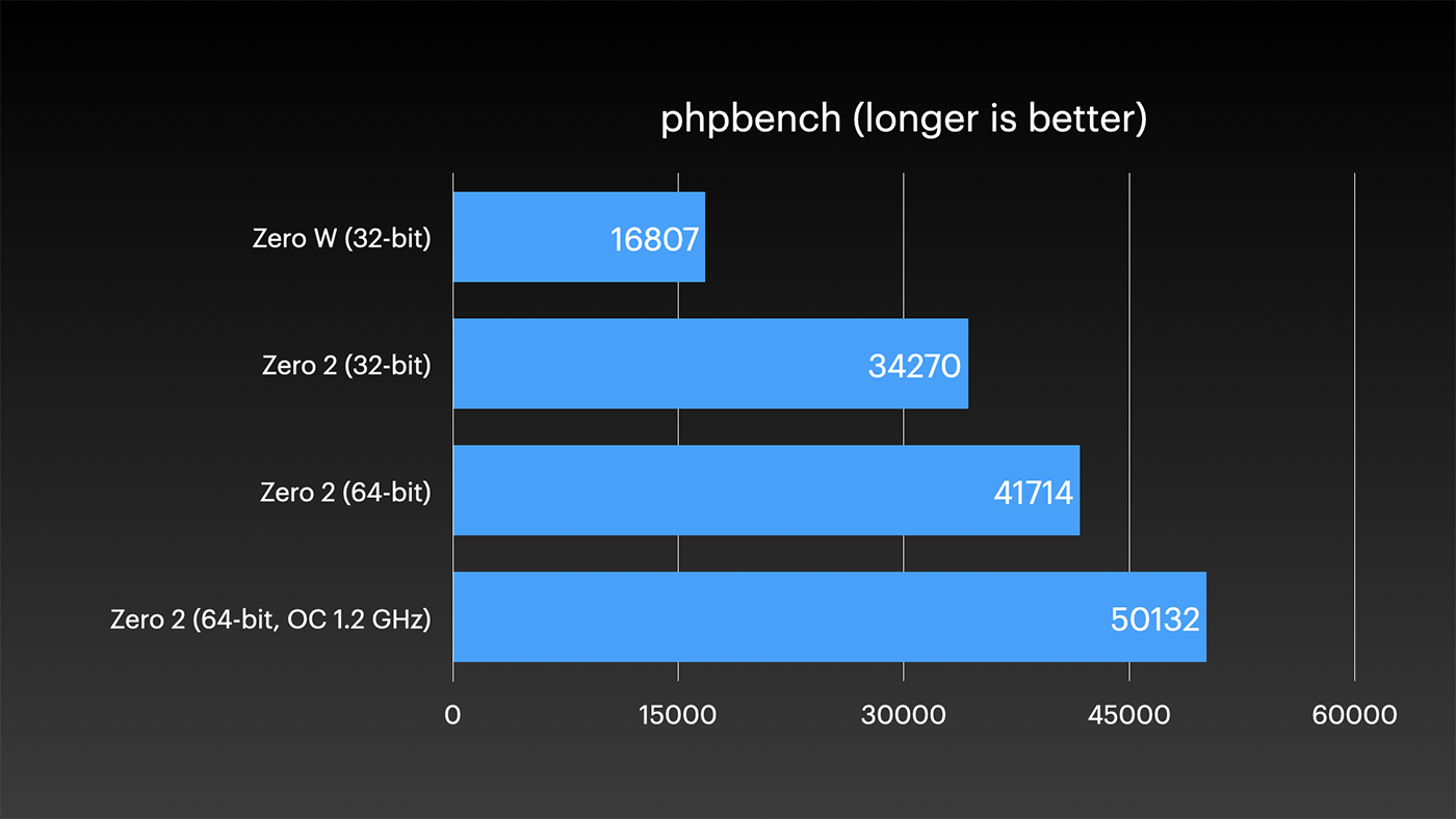
You can expect everything to run at least twice as fast, sometimes 3-4x faster, on the Pi Zero 2 W with it's quad-core A53 chip. But RAM is definitely a limiting factor for many uses.
Two other things I tested were networking performance—since the upgraded CPU can make a difference there—and power consumption:
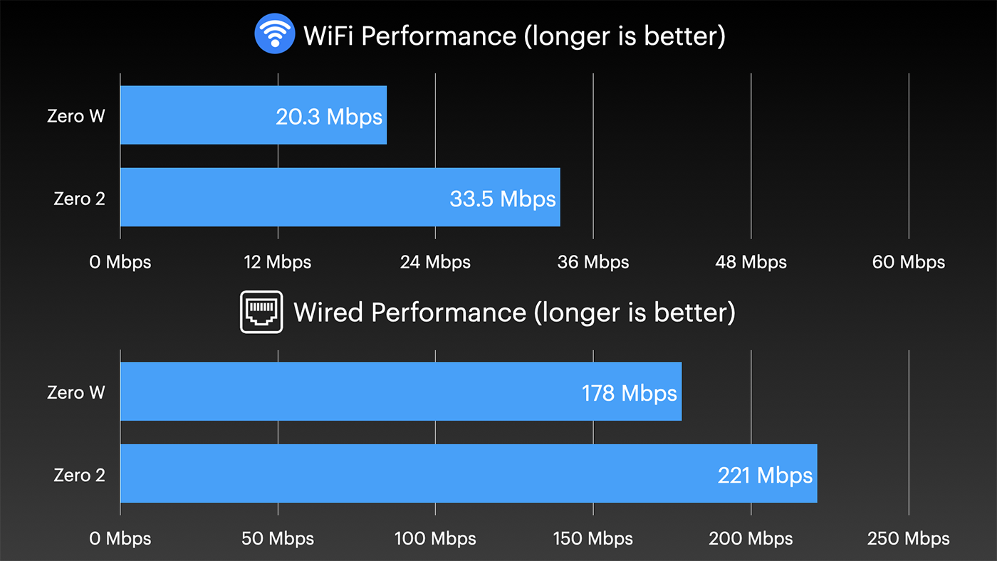
WiFi is about twice as fast, and Wired LAN performance with a Gigabit USB Ethernet adapter is about 25% faster. I should note that it still pales in comparison to the Pi 4, which doubles WiFi performance again, and has built-in 1 Gbps Ethernet!
Finally, here's power consumption as measured by a PowerJive USB power meter.
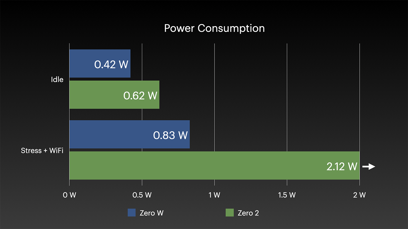
If you turn off almost everything on the Pi Zero to reduce power consumption, you can get the Zero 2 W down to about 100 mA, or 0.52W. The original Zero W could get down to about 80 mA, or 0.42W.
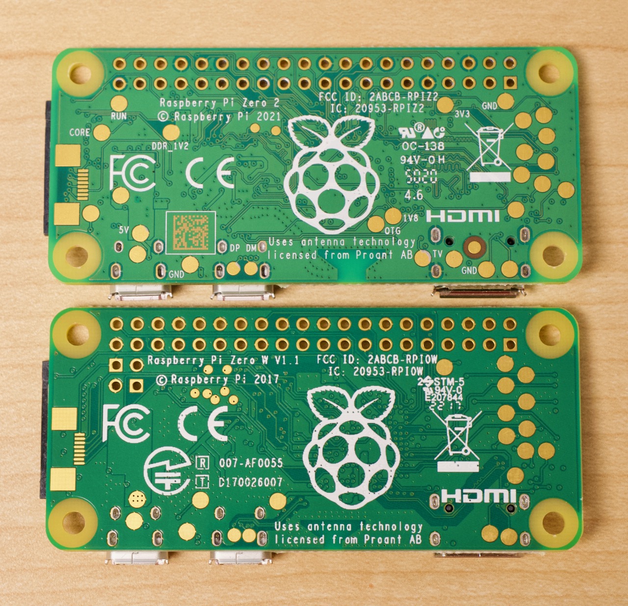
Back side pads
On the back of the Pi Zero 2 W, there are a number of unlabeled pads that can be tapped into for things like composite video output or USB via pogo pins. Unlike the rest of the board's physical layout, the layout of these pads has changed a bit, so some gear that relied on those pads being in a specific location will need to be changed.
Here's a simple image showing the pad locations with the Zero 2 W on top, and the Zero W on bottom:
Conclusion
The Zero 2 W is a nice upgrade over the Zero W, and makes some uses—like retro gaming or light duty tasks—a lot less painful. It's still no performance champ compared to the Pi 4, but it comes in with good features for a still-low price, and I can imagine it'll be hard to find one in stock for some time!
I'll be back next week with details on how I integrated the Pi Zero 2 W in a Null 2 RetroPie gaming handheld build, so be sure to subscribe on YouTube and subscribe to this blog's RSS feed!
And if you haven't yet, go watch the full YouTube review of the Raspberry Pi Zero 2 W.
Recommend
About Joyk
Aggregate valuable and interesting links.
Joyk means Joy of geeK