

6502 “Illegal” Opcodes Demystified
source link: https://www.masswerk.at/nowgobang/2021/6502-illegal-opcodes
Go to the source link to view the article. You can view the picture content, updated content and better typesetting reading experience. If the link is broken, please click the button below to view the snapshot at that time.

6502 “Illegal” Opcodes Demystified
June 5, 2021A closer look at the “illegal” opcodes and undocumented instructions of the MOS 6502 MPU.
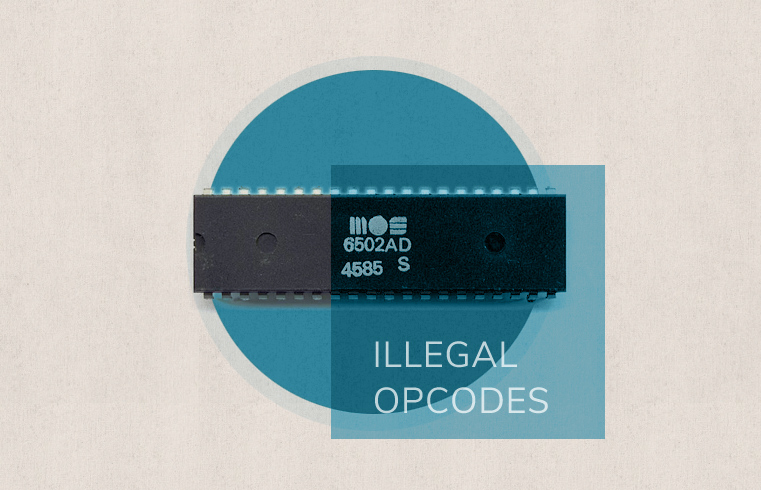
The instruction table of the MOS 6502 MPU, designed by MOS Technology and introduced in 1975 (the CMOS version, 65C02, was developed by Western Design Center) has some obvious gaps, with just 56 intructions documented in various address modes. This leaves 105 undocumented slots — and the 6502 community has been eager to fill these gaps, ever since.
Still, there’s some mystery left and there are questions unanswered, like, were at least some of them intentional (especially, since some of them are handy for block transfer, something the Z80 has dedicated instructions for) or are they all by accident, how do they behave, and why so? Here, we’ll try to come up with some answers to these questions.
First, let's have a look at the instruction table, as it is commonly presented, with the blank gaps filled in. (Here, for the “illegal” opcodes, we use the mnemonics used by the DASM and ACME assemblers, with the exception of “USBC” for instruction code $EB, where these use plain “SBC”.)
 Instruction set of the MOS 6502 MPU, “illegals” on grey background. — Open in a new tab.
And here are all the 21 (more or less) “illegal” opcodes (alternative names given in parentheses) as they are commonly described:
ALR (ASR)
AND oper + LSR
A AND oper, 0 -> [76543210] -> C
addressingassembleropcbytescyclesimmediateALR #oper4B22
ANC
AND oper + set C as ASL
A AND oper, bit(7) -> C
addressingassembleropcbytescyclesimmediateANC #oper0B22
ANC (ANC2)
AND oper + set C as ROL
effectively the same as instr. 0B
A AND oper, bit(7) -> C
addressingassembleropcbytescyclesimmediateANC #oper2B22
ANE (XAA)
* AND X + AND oper
Highly unstable, do not use.A base value in A is determined based on the contets of A and a constant, which may be typically $00, $ff, $ee, etc. The value of this constant depends on temerature, the chip series, and maybe other factors, as well.
In order to eliminate these uncertaincies from the equation, use either 0 as the operand or a value of $FF in the accumulator.
(A OR CONST) AND X AND oper -> A
addressingassembleropcbytescyclesimmediateANE #oper8B22 ††
ARR
AND oper + ROR
This operation involves the adder:
V-flag is set according to (A AND oper) + oper
The carry is not set, but bit 7 (sign) is exchanged with the carry
A AND oper, C -> [76543210] -> C
addressingassembleropcbytescyclesimmediateARR #oper6B22
DCP (DCM)
DEC oper + CMP oper
M - 1 -> M, A - M
addressingassembleropcbytescycleszeropageDCP operC725 zeropage,XDCP oper,XD726 absoluteDCP operCF36 absolut,XDCP oper,XDF37 absolut,YDCP oper,YDB37 (indirect,X)DCP (oper,X)C328 (indirect),YDCP (oper),YD328
ISC (ISB, INS)
INC oper + SBC oper
M + 1 -> M, A - M - C -> A
addressingassembleropcbytescycleszeropageISC operE725 zeropage,XISC oper,XF726 absoluteISC operEF36 absolut,XISC oper,XFF37 absolut,YISC oper,YFB37 (indirect,X)ISC (oper,X)E328 (indirect),YISC (oper),YF324
LAS (LAR)
LDA/TSX oper
M AND SP -> A, X, SP
addressingassembleropcbytescyclesabsolut,YLAS oper,YBB34*
LAX
LDA oper + LDX oper
M -> A -> X
addressingassembleropcbytescycleszeropageLAX operA723 zeropage,YLAX oper,YB724 absoluteLAX operAF34 absolut,YLAX oper,YBF34* (indirect,X)LAX (oper,X)A326 (indirect),YLAX (oper),YB325*
LXA (LAX immediate)
Store * AND oper in A and X
Highly unstable, involves a 'magic' constant, see ANE
(A OR CONST) AND oper -> A -> X
addressingassembleropcbytescyclesimmediateLXA #operAB22 ††
RLA
ROL oper + AND oper
M = C <- [76543210] <- C, A AND M -> A
addressingassembleropcbytescycleszeropageRLA oper2725 zeropage,XRLA oper,X3726 absoluteRLA oper2F36 absolut,XRLA oper,X3F37 absolut,YRLA oper,Y3B37 (indirect,X)RLA (oper,X)2328 (indirect),YRLA (oper),Y3328
RRA
ROR oper + ADC oper
M = C -> [76543210] -> C, A + M + C -> A, C
addressingassembleropcbytescycleszeropageRRA oper6725 zeropage,XRRA oper,X7726 absoluteRRA oper6F36 absolut,XRRA oper,X7F37 absolut,YRRA oper,Y7B37 (indirect,X)RRA (oper,X)6328 (indirect),YRRA (oper),Y7328
SAX (AXS, AAX)
A and X are put on the bus at the same time (resulting effectively in an AND operation) and stored in M
A AND X -> M
addressingassembleropcbytescycleszeropageSAX oper8723 zeropage,YSAX oper,Y9724 absoluteSAX oper8F34 (indirect,X)SAX (oper,X)8326
SBX (AXS, SAX)
CMP and DEX at once, sets flags like CMP
(A AND X) - oper -> X
addressingassembleropcbytescyclesimmediateSBX #operCB22
SHA (AHX, AXA)
Stores A AND X AND (high-byte of addr. + 1) at addr.
unstable: sometimes 'AND (H+1)' is dropped, page boundary crossings may not work (with the high-byte of the value used as the high-byte of the address)
A AND X AND (H+1) -> M
addressingassembleropcbytescyclesabsolut,YSHA oper,Y9F35 †(indirect),YSHA (oper),Y9326 †
SHX (A11, SXA, XAS)
Stores X AND (high-byte of addr. + 1) at addr.
unstable: sometimes 'AND (H+1)' is dropped, page boundary crossings may not work (with the high-byte of the value used as the high-byte of the address)
X AND (H+1) -> M
addressingassembleropcbytescyclesabsolut,YSHX oper,Y9E35 †
SHY (A11, SYA, SAY)
Stores Y AND (high-byte of addr. + 1) at addr.
unstable: sometimes 'AND (H+1)' is dropped, page boundary crossings may not work (with the high-byte of the value used as the high-byte of the address)
Y AND (H+1) -> M
addressingassembleropcbytescyclesabsolut,XSHY oper,X9C35 †
SLO (ASO)
ASL oper + ORA oper
M = C <- [76543210] <- 0, A OR M -> A
addressingassembleropcbytescycleszeropageSLO oper0725 zeropage,XSLO oper,X1726 absoluteSLO oper0F36 absolut,XSLO oper,X1F37 absolut,YSLO oper,Y1B37 (indirect,X)SLO (oper,X)0328 (indirect),YSLO (oper),Y1328
SRE (LSE)
LSR oper + EOR oper
M = 0 -> [76543210] -> C, A EOR M -> A
addressingassembleropcbytescycleszeropageSRE oper4725 zeropage,XSRE oper,X5726 absoluteSRE oper4F36 absolut,XSRE oper,X5F37 absolut,YSRE oper,Y5B37 (indirect,X)SRE (oper,X)4328 (indirect),YSRE (oper),Y5328
TAS (XAS, SHS)
Puts A AND X in SP and stores A AND X AND (high-byte of addr. + 1) at addr.
unstable: sometimes 'AND (H+1)' is dropped, page boundary crossings may not work (with the high-byte of the value used as the high-byte of the address)
A AND X -> SP, A AND X AND (H+1) -> M
addressingassembleropcbytescyclesabsolut,YTAS oper,Y9B35 †
USBC (SBC)
SBC oper + NOP
effectively same as normal SBC immediate, instr. E9.
A - M - C -> A
addressingassembleropcbytescyclesimmediateUSBC #operEB22
NOPs (including DOP, TOP)
Instructions effecting in 'no operations' in various address modes. Operands are ignored.
opcaddressingbytescycles1Aimplied12 3Aimplied12 5Aimplied12 7Aimplied12 DAimplied12 FAimplied12 80immediate22 82immediate22 89immediate22 C2immediate22 E2immediate22 04zeropage23 44zeropage23 64zeropage23 14zeropage,X24 34zeropage,X24 54zeropage,X24 74zeropage,X24 D4zeropage,X24 F4zeropage,X24 0Cabsolute34 1Cabsolut,X34* 3Cabsolut,X34* 5Cabsolut,X34* 7Cabsolut,X34* DCabsolut,X34* FCabsolut,X34*
JAM (KIL, HLT)
These instructions freeze the CPU.
The processor will be trapped infinitely in T1 phase with $FF on the data bus. — Reset required.
Instruction codes: 02, 12, 22, 32, 42, 52, 62, 72, 92, B2, D2, F2
Legend to markers used in the instruction details:
* add 1 to cycles if page boundery is crossed †unstable ††highly unstableDisclaimer:
Information is provided as-is, without any guarantee of completness or correctness.
None of these “illegal” instructions are guaranteed to work, some are highly unstable, some may even start two asynchronous threads competing in race condition with the winner determined by such miniscule factors as temperature or minor differences in the production series, at other times, the outcome depends on the exact values involved and the chip series.
Use with care and at your own risk.
Well, this is all fine and good, but… we really do not learn much about hat they are and why these are.
Let’s risk another look at the instruction layout, as it ought to be viewed.
Another Look at the Instruction Layout
The 6502 instruction table is laid out according to a pattern a-b-c, where
a and b are an octal number each, followed by a group of two binary digits c,
as in the bit-vector “aaabbbcc”.
aaabbbccbit76543210(0…7)(0…7)(0…3)
Example:
All ROR instructions share a = 3 and c = 2 (3b2) with the address mode in b.
At the same time, all instructions addressing the zero-page share b = 1 (a1c).
abc = 312 => ( 3 << 5 | 1 << 2 | 2 ) = %011.001.10 = $66 “ROR zpg”.
If we arrange the instruction table by components c, a and b, we find them all neatly lined up per address mode in the vertical columns (with the notable exception of instructions related to the X register, which show up with their respective Y counterpart for address modes involving an index by X). Notably, all the “illegals” adhere strictly to this scheme.
Moreover, all the instructions internal to the CPU and its flow of control are listed in the top quarter at c=0, while the bottom quarter at c=3, where we find the majority of “illegal” opcodes, is completely unpopulated by official opcodes. Further, for sections, where c=1 or c=2, we see opcodes of a kind sharing the same row (with the notable outliers of the two stack transfer instructions “TXS” and TSX).
 Instruction layout of the MOS 6502 MPU, “illegals” on grey background. — Open in a new tab.
While this certainly informative, it still doesn’t give away a systemic aspect of the unimplemented instructions, nor does this view tell us what they really are.
So let’s give this another try, this time arranging the instruction layout by components a, c and b:
 Structured view of the 6502 instruction layout, “illegals” on grey background. — Open in a new tab.
Well, this is better, much better.
First, we learn what the additional NOPs really are. By comparing opcodes by row and address modes by column, we can clearly see, what these ought to be.
E.g.,
$80 (a=4, c=0, b=0) is clearly “STY immediate”, attempting to store the the contents of the Y register in the literal operand.
Generally speaking, these additional NOPs are instructions with non-functional or nonsensical address modes, which do execute, but without any external effects.
However, instructions of this group which involve indirect addressing fail entirely with the CPU infinitely trapped in T1 phase, resulting in a “JAM” (or KIL), rendering the CPU unresponsive and requiring a reset.
Instructions at ‘C = 3’
This is the really interesting part, the meat of the “illegal opcodes”.
Generally, we may observe that any of the instructions at c=3 are really inheriting their behavior from those at c=1 and c=2 in the same slot, found in the rows immediately above, same column, using the address mode of the instruction at c=1. Mind that in binary 3 is the composite of 1 and 2 with bits 0 and 1 set.
In other words, any instruction xxxxxx11 will execute the instructions at xxxxxx01 and xxxxxx10 at once, using the address mode of the instruction at xxxxxx01. (However, the general rule regarding X and Y register specific indexed address modes still applies.)
E.g.,
“SAX abs” ($8F, a=4,c=3,b=3) is the composite of
“STA abs” ($8D, a=4,c=1,b=3) and
“STX abs” ($8E, a=4,c=2,b=3).
E.g.,
“LAX X,ind” ($A3, a=5,c=3,b=0) is the composite of
“LDA X,ind” ($A1, a=5,c=1,b=0) and
“LDX imm” ($A2, a=5,c=2,b=0).
The “Magic” Constant
Let’s have a closer look at the two highly unstable instructions “ANE” (XAA) and “LXA” (LAX immediate) involving a “magic constant” — typically $00, $FF, $EE, etc. —, which are both combinations of an accumulator operation and an inter-register transfer between the accumulator and the X register:
$8B (a=4,c=3,b=2): ANE imm = STA imm (NOP) + TXA
                   (A OR CONST) AND X AND oper -> A

$AB (a=5,c=3,b=2): LXA imm = LDA imm + TAX
                   (A OR CONST) AND oper -> A -> X
In the case of “ANE”, the contents of the accumulator is put on the internal
data lines at the same time as the contents of the X-register, while there's
also the operand read for the immediate operation, with the result
transferred to the accumulator.
In the case of “LXA”, the immediate operand and the contents of the accumulator
are competing for the imput lines, while the result will be transferred to
both the accumulator and the X register.
The outcome of these competing, noisy conditions depends on the production
series of the chip, and maybe even on environmental conditions. This effects
in an OR-ing of the accumulator with the “magic constant” combined with an
AND-ing of the competing inputs. The final transfer to the target register(s)
then seems to work as may be expected.
(We may note that all the instructions involved in these two opcodes complete in 2 cycles, the shortest sequence available on the 6502, meaning, everything is virtually happening “at once”.)
This AND-ing of competing output values suggests that the 6502 is working internally
in active low logic, where all data lines are first set to high and then
cleared for any zero bits. This also suggests that the “magic constant” stands
merely for a partial transfer of the contents of the accumulator.
(Mind that this is not a qualified statement about the internals of the 6502 hardware, but merely an observation on its external effects.)
Much of this also applies to “TAS” (XAS, SHS), $9B, but here the extra cycles
for indexed addressing seem to contribute to the conflict being resolved
without this “magic constant”. However, “TAS” is still unstable.
The ‘H+1’ Group
There are four instructions, which add the peculiar term ‘high-byte of provided address + 1’ to the equation. These are:
SHA (AHX, AXA)       A AND X AND (H+1) -> M
                     $9F  SHA abs,Y  (5)

SHX (A11, SXA, XAS)  X AND (H+1) -> M
                     $9E  SHX abs,Y  (5)

SHY (A11, SYA, SAY)  Y AND (H+1) -> M
                     $9C  SHY abs,X  (5)

TAS (XAS, SHS)       A AND X -> SP, A AND X AND (H+1) -> M
                     $9B  TAS abs,Y  (5)
We may already see, where this comes from: as the calculations for the effective address involves the ALU, a partial result for the high-byte adds to the conflicting output values. However, depending on minor timing discrepancies, this term may be also dropped (meaning, become overriden).
We may also discern, why the effective high-address may be replaced by the ouput value altogether, in case a page boundary is crossed, since this provides just the extra amount of timing required to allow the output value to stabilize and to override the address high-byte. Again, these instructions are unstable.
The Outliers
We may note that “SHY” and “SHX” are not part of the c=3 group, but rather the unimplemented instructions “STY abs,X” (c=0) and “STX abs,Y” (c=2) respectively. Both are apparently falling back to the implementation of “STA abs,X” with the extra quirk of the ‘H+1’ term.
“SHA abs,Y”, finally, is the composite instruction adhering to the c=3 rule that we have already established, executing “STA abs,X” and “SHX abs,Y” at once. (Notably, this flips the address mode to “abs,Y”, where “abs,X” may be expected. Which suggests that this adjustment for indexed instructions concerning any X register transfers is implemented as an additional stage.)
“SHA ind,Y” ($93), however, is the composite of “STA ind,Y” ($91) and “SHX ind,Y” ($92), which JAMs on its own.
Mysterious NOPs
As mentioned earlier, we are able to figure out, what most of the NOPs and JAM instructions are, just from their disposition on the layout. But there is a group of 12 NOP instructions (all at a=0 and c≤3 and odd values of b), which seem to be truly empty slots. Namely these are the instructions at:
$04 (a=0, c=0, b=1)
$0C (a=0, c=0, b=3)
$14 (a=0, c=0, b=5)
$1C (a=0, c=0, b=7)
$34 (a=1, c=0, b=5)
$3C (a=1, c=0, b=7)
$44 (a=2, c=0, b=1)
$54 (a=2, c=0, b=5)
$5C (a=2, c=0, b=7)
$64 (a=3, c=0, b=1)
$74 (a=3, c=0, b=5)
$7C (a=3, c=0, b=7)
From their very position on the instruction layout, we may infer that these should be instructions internal to the CPU. Typically, instructions at (a=0/c=0) have a counterpart at (a=1/c=0) in the repective b position, as is also true for (a=2/c=0) and (a=3/c=0). E.g., PHP & PLP, BPL & BMI, CLC & SEC, and so on.
Here, however, the counterparts are missing, as well. (Only $04 and $0C have a counterpart in “BIT”, but we may have a hard time figuring out, what the counterpart of “BIT” may actually be.) For all we know, these instructions are simply unimplemented, and it’s a small wonder that the timing sequence for these instructions does resolve without a JAM. But these instructions are still interesting, as they direct our attention towards how the internal instructions which are implemented are systematically arranged on the decoding matrix.
The same pattern, BTW, may be observed for most instructions, so that we may think of even and consecutive odd values of a and same values for c and b as “opposing” or “complementary” slots, where we find in one slot the store instruction for a given register in and the other one the load instruction, both in the address mode defined by b, or a shift in one direction and the opposing shift in the other direction.
Conclusions
What we have observed here is really a text-book example of undefined behavior for undefined input patterns. For any instruction with the two least significant bits set at once (c=3) the two instructions in the respective slot with c=1 and c=2 are started in parallel, asynchronous threads with competing output values AND-ed. Minor implementation details and environmental factors may contribute to the outcome of some of these instructions and how the timing eventually stabilizes.
Notably, there are no NOPs or jamming instructions at c=3, meaning, it doesn't matter, if any of the two threads JAMs, if the timing for one of them resolves successfully (thus advancing the internal phase).
At c=0, c=1 and c=2 we find either undocumented instructions with ineffective address modes, or undocumented instructions that fail entirely over unresolved timing issues, resulting in a “JAM”. There are just two exceptions to this rule, namely “SHY” and “SHX”, which, while unstable, may be somewhat usable.
So is any of this intentional? Hardly. It’s just undefined behavior. Orderly chaos as provided by the decoding matrix. However, we may learn some from this about the internals of 6502 and its various close cousins. — Which is at least some.
Mind that there is much more competent commentary on the 6502, which is based on analysis of the actual hardware, especially at visual6502.org. But, maybe, you found this “hermeneutic” approach, trying to reveal the systematic aspects of what may be observed externally, interesting, as well.

PS: All the tables in this post are SVG images. You may download and use them (mind the “open in a new tab” links), but please give reference to https://www.masswerk.at/6502/6502_instruction_set.html, where you can find the original tables.
Norbert Landsteiner,
Vienna, 2021-06-05
Recommend
About Joyk
Aggregate valuable and interesting links.
Joyk means Joy of geeK